Skip to the content
PCBKitNew board
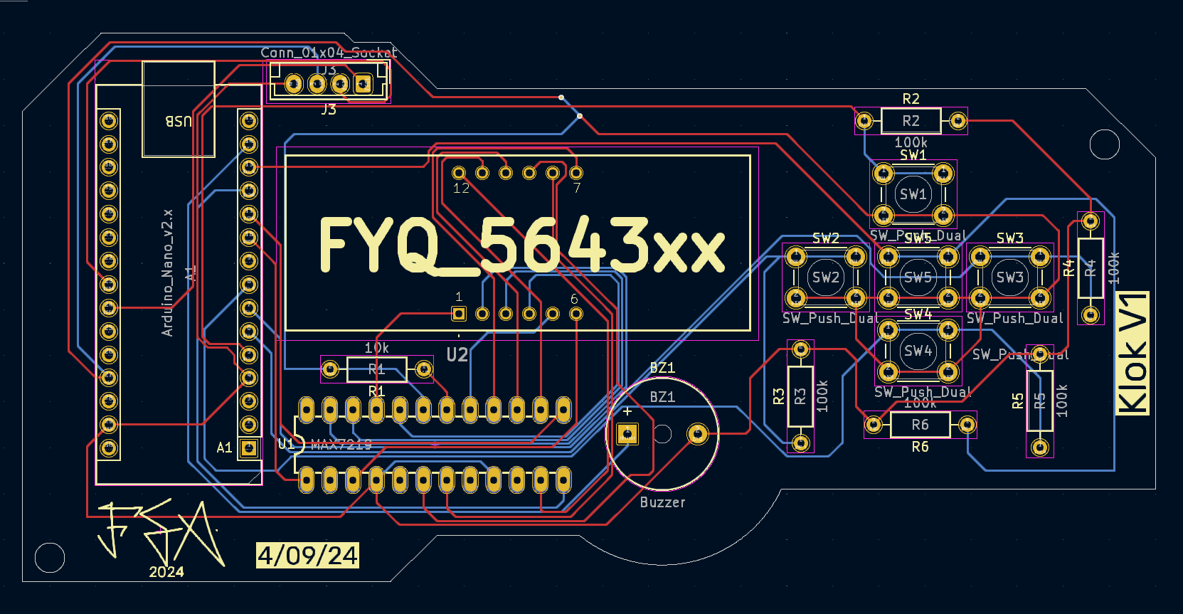
2 layers123 × 59.5 mmV1 PCB, the printed circuit board in 3D

A clock, minimalist, with the features and improvements I want to.

Size
123 × 59.5 mm
Copper layers
2
Thickness
1.6 mm
Parts
22
Nets
47
Pads
114
Tracks, vias
308, 3
Routed
Yes
KiCad
KiCad 8.0 (file 20240108)
Created
5 Sep 2024
Updated
7 Jan 2026

Overview

V1 PCB is an open-source printed circuit board by fgutep, from the fgutep/Klok repository on GitHub, published under the MIT licence. It is a 2-layer board of 123 × 59.5 mm with 22 parts on 47 nets, routed with 308 tracks and 3 vias.

It is built around the MAX7219M. Its parts include 9 resistors, 5 switches, 3 connectors and 2 ICs. It belongs with the AVR (ATmega, ATtiny) boards of this library.

Main components

1

README

README.md

Klok

Klok is a cyberpunk-inspired alarm clock that rejects the idea that electronics should be hidden.
Instead of plastic shells and invisible circuitry, Klok puts the PCB, components, and imperfections front and center.

This project is as much about design philosophy and learning through failure as it is about telling time.


Concept

Most digital clocks try to disappear.
Klok does the opposite.

  • Exposed traces instead of hidden wiring
  • Bulky through-hole components instead of flat SMD minimalism
  • A visible Arduino Nano instead of a sealed SoC
  • A non-rectangular PCB framed as an object, not a board

The result is a clock that looks unfinished on purpose—industrial, crude, and honest.


Design Philosophy

Embrace Rawness

  • Do not hide electronic components
  • Let depth, height, and shadows exist
  • Celebrate through-hole parts and hand-assembled character
  • Treat the PCB as the product, not something to be enclosed

Frame, Don’t Conceal

  • Custom PCB outline breaks away from rectangular norms
  • Enclosure adapts to the board, not the other way around

Features (Intended – V1)

  • 4-digit 7-segment display driven by MAX7219
  • Alarm functionality via piezo buzzer
  • Auto-dimming using photoresistor + PWM
  • 5-button control interface in cross layout
  • RTC support via external I2C module (JST)
  • LiPo-ready power input with external BMS support

⚠️ See Known Issues — not all features work in V1.


Hardware Overview

Core Components

  • Arduino Nano (ATmega328P)
  • MAX7219 LED driver
  • Common-anode 4-digit 7-segment display
  • Photoresistor with voltage divider
  • Piezo buzzer
  • 5× tactile switches (software debounced)
  • 2× JST connectors:
    • J1: Power input (1S LiPo + BMS)
    • J2: I2C (RTC module)

PCB

  • Version: V1.0
  • Two-layer PCB
  • Exposed component aesthetic
  • Custom non-rectangular outline

PCB Image


Known Issues — V1 (Critical)

⚠️ This version is non-functional and should not be manufactured.

1. I2C Connector (J2) — Completely Disconnected

  • SDA, SCL, VCC, and GND traces failed during manufacturing
  • Caused by:
    • Acid traps
    • No teardrops
    • Large manufacturing tolerances
  • Result:
    RTC cannot communicate → clock cannot keep time

2. Fourth Display Digit Not Updating

  • Last digit (minutes) does not respond
  • Issue persists even after manual trace jumping
  • Possible causes:
    • Severe pull-up / pull-down fault on MAX7219 input
    • Partial internal damage to the MAX7219 output stage

Status:
V1 is a learning artifact, not a working device.


Lessons Learned

This was my third densely populated two-layer PCB, and it shows.

Key mistakes:

  • No teardrops on critical traces
  • Poor routing created acid traps
  • Manufacturing tolerances not accounted for
  • Non-socketed MAX7219 made debugging nearly impossible
  • External RTC dependency introduced a single point of failure

Despite this, the concept, interaction model, and visual identity are solid.


Roadmap — V2 (Planned)

  • Replace Arduino Nano with ESP32
  • Wi-Fi NTP time sync (no external RTC)
  • Proper routing with teardrops and best practices
  • Socketed MAX7219 for debugging and replacement
  • Clean power architecture:
    • 5V for LEDs
    • 3.3V for MCU
  • Enclosure designed alongside PCB, not after

Repository Structure

text
.
├── V1 PCB/ # PCB files for first revision
├── Arduino-Notes/ # Firmware notes and experiments
├── img/ # Renders and PCB images

This repository exists to document the design, mistakes, and evolution of Klok. Klok comes from the Dutch / German word for “clock” — simple, direct, functional.
Much like the object itself.

Parts

22
QtyValueFootprintReferences
7100kResistor_THT:R_Axial_DIN0207_L6.3mm_D2.5mm_P10.16mm_HorizontalR2, R3, R4, R5, R6, R8, R9
5SW_Push_DualButton_Switch_THT:SW_PUSH_6mmSW1, SW2, SW3, SW4, SW5
2Conn_01x02_SocketConnector_JST:JST_EH_B2B-EH-A_1x02_P2.50mm_VerticalJ1, Snooze1
110kResistor_THT:R_Axial_DIN0207_L6.3mm_D2.5mm_P10.16mm_HorizontalR1
1Arduino_Nano_v2.xModule:Arduino_NanoA1
1BuzzerBuzzer_Beeper:Buzzer_12x9.5RM7.6BZ1
1Conn_01x04_SocketConnector_JST:JST_EH_B4B-EH-A_1x04_P2.50mm_VerticalJ3
1LOGOLOGOG***
1MAX7219MAX7219:DIL24U1
1R_PhotoOptoDevice:R_LDR_D6.4mm_P3.4mm_VerticalR7
1~CostumScreen:FYQ_5643xxU2

Questions

How big is the V1 PCB PCB?

It measures 123 × 59.5 mm and has 2 copper layers, 1.6 mm thick.

What parts does the V1 PCB use?

22 parts, built around the MAX7219M. The full list of its parts is on this page, with links to each part's symbol and footprint where PCBKit's library has them.

Where can I download the V1 PCB KiCad files?

From the fgutep/Klok repository on GitHub, at the commit this page was made from: the board is V1 PCB/V1.kicad_pcb and its schematic V1 PCB/V1.kicad_sch. PCBKit opens the board in the browser, with nothing to install.

Can I use the V1 PCB design in my own project?

Its repository publishes it under the MIT licence: you may reuse it on that licence's terms (keep the author's notice, and for a copyleft licence share your changes alike).

Similar boards

  • 2 layers181 × 97 mmOpenDeck r3.1.2, the printed circuit board in 3D

    OpenDeck r3.1.2

    shanteacontrols/OpenDeck

    A platform for building interactive control and sensing devices using MIDI and OSC built with Zephyr RTOS.

    262 parts960Apache-2.0
  • 2 layers482.6 × 35.6 mmPrecision clock, the printed circuit board in 3D

    Precision clock

    mitxela/PrecisionClock-Hardware

    PCB design for the Precision Clock Mk III

    49 parts41
  • 2 layers85.6 × 41 mmHl alyx glove, the printed circuit board in 3D

    Hl alyx glove

    StarGate01/hl-alyx-glove

    Firmware and Hardware for a Half-Life: Alyx Gravity Glove Replica

    38 parts21MIT
  • 2 layers542.3 × 27.3 mmGlowboardng, the printed circuit board in 3D

    Glowboardng

    Eigenbaukombinat/glowboard

    The Glowboard Plotter plots images using 64 UV LEDs attached in a line moved over a 120cmx60cm glow-in-the-dark sheet by a stepper.

    69 parts6
  • 2 layers70 × 50.1 mmDoom clock, the printed circuit board in 3D

    Doom clock

    stecman/avr-doomclock

    GPS clock on an ATTiny with MAX7219 7-segment driver

    24 parts5MIT
  • 2 layers91.4 × 119.4 mmPainel pcb1, the printed circuit board in 3D

    Painel pcb1

    ArqueologiaDigital/PatinhoFeio_Painel_KICAD

    63 parts4
  • 2 layers142.2 × 64.4 mmFcu mb, the printed circuit board in 3D

    Fcu mb

    VirtualGit/HomeCockpitA320

    A320 Home Cockpit project

    69 parts4