2 layers103 × 30.5 mm

 Fern518/Chesters-Hackpad
My personal macropad for media control. Features an OLED display and encoder knob for visualising music and volume control, and six addtional keys for useful shortcuts.
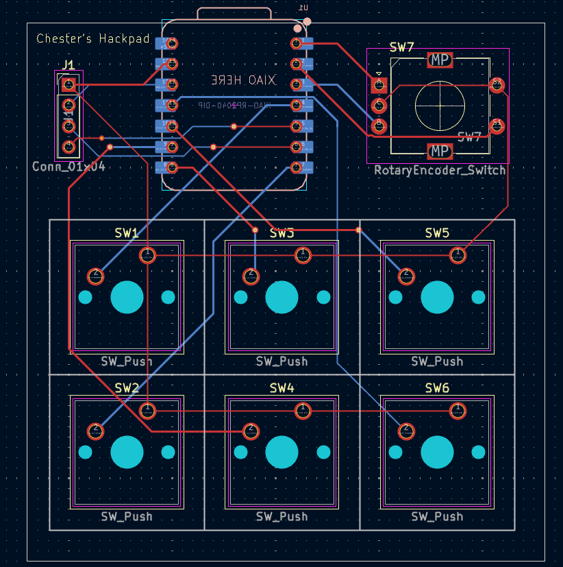
Hackpad is an open-source printed circuit board by Fern518, from the Fern518/Chesters-Hackpad repository on GitHub. It is a 2-layer board of 63.5 × 66 mm with 9 parts on 14 nets, routed with 62 tracks and 6 vias.
Its parts include 7 switches, 1 IC and 1 connector. It belongs with the lEDs and displays and keyboards and input boards and the RP2040 boards of this library.
A custom PCB-based macropad built for the Hack Club Blueprint program.
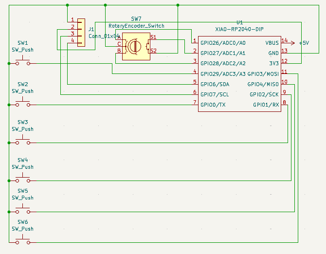
It functions as a miniature media dashboard: the display shows the current track (TO BE IMPLEMENTED), the knob controls volume, and the six keys can be bound to any shortcut.
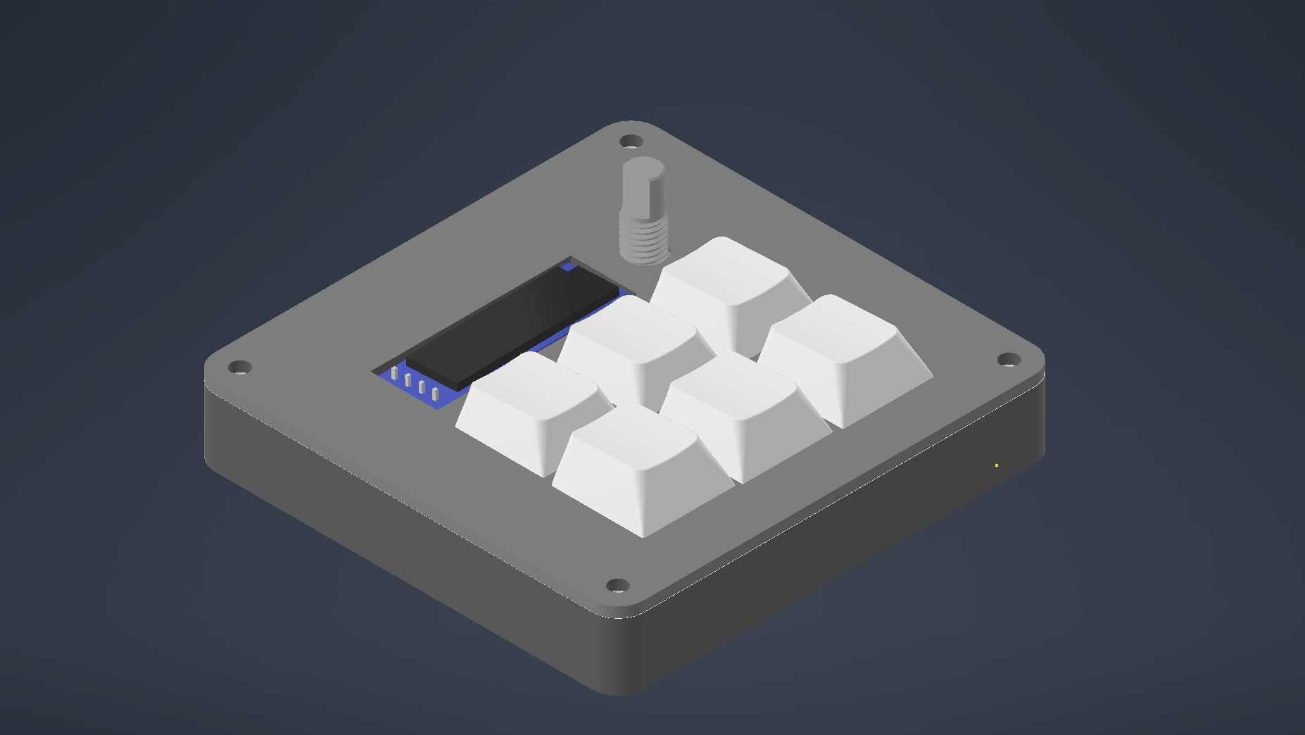 Everything fits together using 4 M3 Bolts and Heatset inserts, one in each corner.
It has 2 separate printed pieces. The base, where the PCB sits, and the top cover, which protects the PCB.
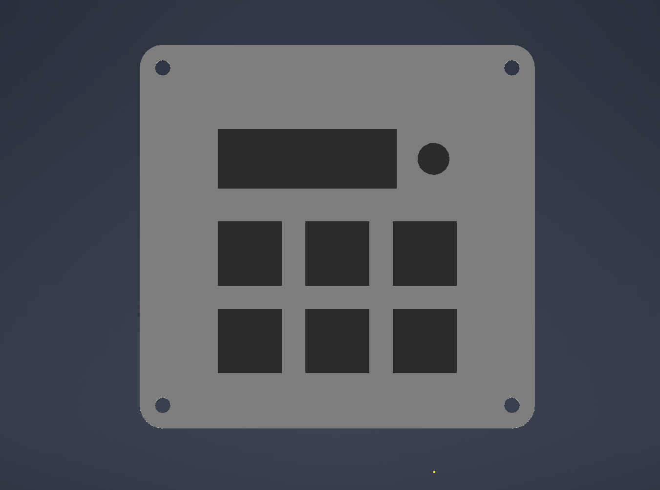
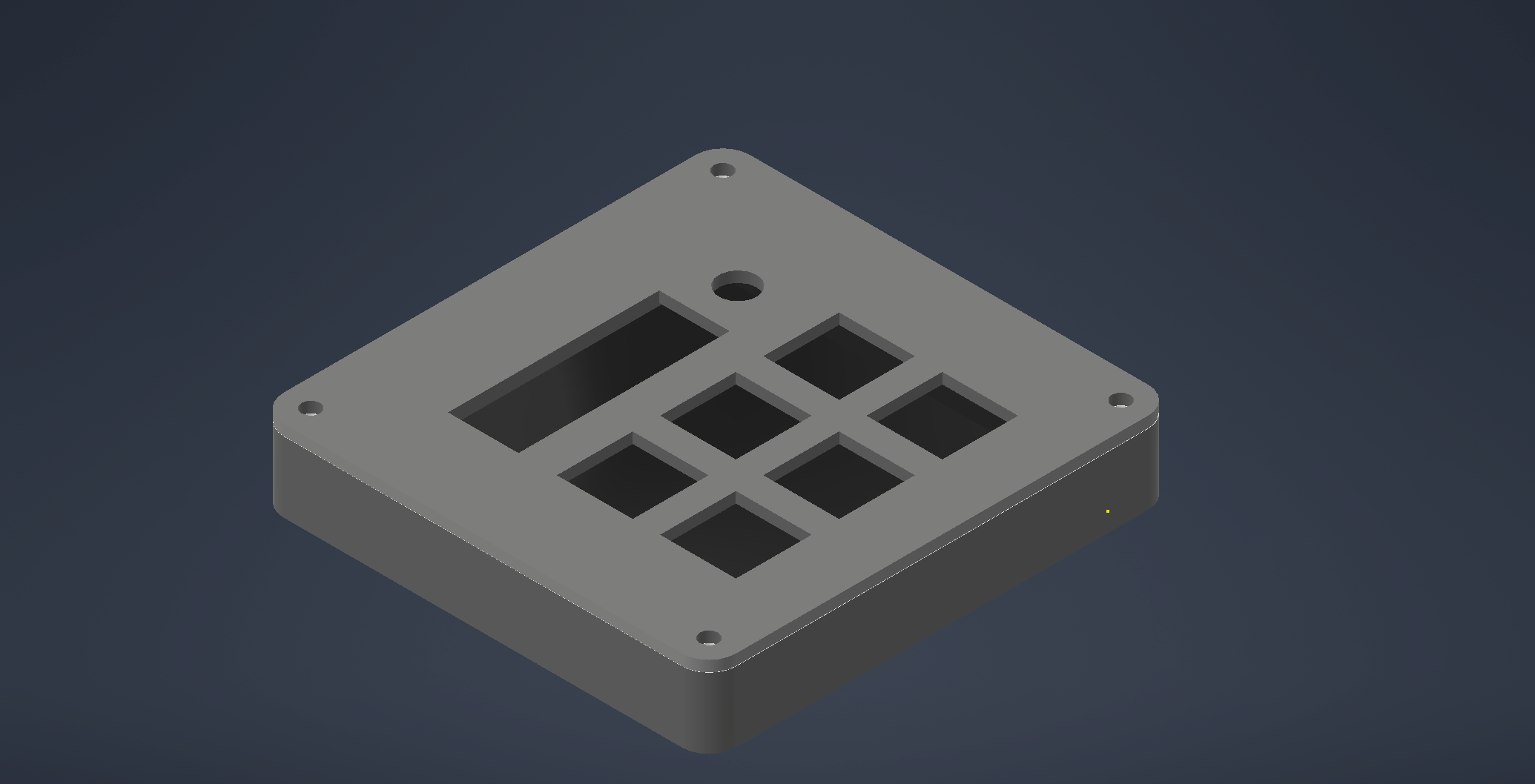
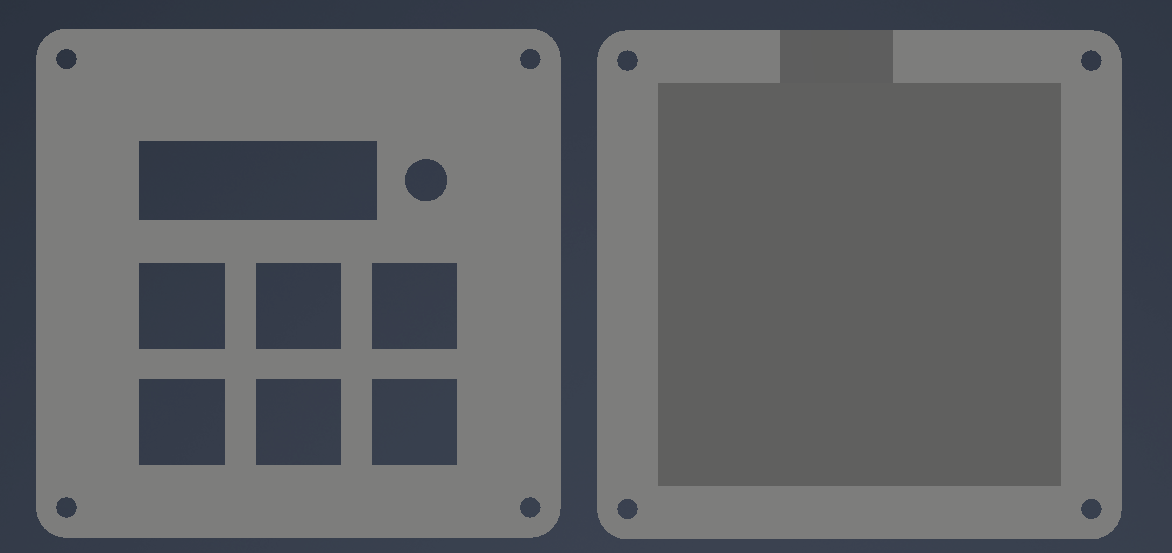
My PCB was designed in KiCad. The XIAO is mounted on the bottom of the PCB to allow space for the OLED display.
Schematic:
PCB:
| Qty | Value | Footprint | References |
|---|---|---|---|
| 6 | SW_Push | Button_Switch_Keyboard:SW_Cherry_MX_1.00u_PCB | SW1, SW2, SW3, SW4, SW5, SW6 |
| 1 | Conn_01x04 | Connector_PinHeader_2.54mm:PinHeader_1x04_P2.54mm_Vertical | J1 |
| 1 | RotaryEncoder_Switch | Rotary_Encoder:RotaryEncoder_Alps_EC11E-Switch_Vertical_H20mm | SW7 |
| 1 | XIAO-RP2040-DIP | OPL:XIAO-RP2040-DIP | U1 |
It measures 63.5 × 66 mm and has 2 copper layers, 1.6 mm thick.
9 parts. The full list of its parts is on this page, with links to each part's symbol and footprint where PCBKit's library has them.
From the Fern518/Chesters-Hackpad repository on GitHub, at the commit this page was made from: the board is PCB/hackpad/hackpad.kicad_pcb and its schematic PCB/hackpad/OPL_Kicad_Library-master/Grove Vision AI V2 Library/Grove - Vision AI Module V2.kicad_sch. PCBKit opens the board in the browser, with nothing to install.
Its repository states no licence, so its author keeps all rights: ask Fern518 before reusing the design.


FrameworkComputer/ExpansionCards
Reference designs and documentation to create Expansion Cards for the Framework Laptop

VoronDesign/Voron-Hardware
Cool Hardware designed by the Voron Design group

hackclub/OnBoard
💡 Join 1,000 teenagers and make your first PCB with a $100 grant!


adamws/kicad-kbplacer
KiCad plugin for automatic keyboard's key placement and routing