4 layers77 × 131.5 mm
FujiNet ChannelF Rev0
FujiNetWIFI/fujinet-hardware
Schematics and design files for FujiNet hardware
106 parts142

 fabPlane/ps1-memory-card-usb
RP2040 PS1 memory card with USB-C and microSD, designed in Fabdesk
Ps1-memory card usb is an open-source printed circuit board by fabPlane, from the fabPlane/ps1-memory-card-usb repository on GitHub, published under the GPL-3.0 licence. It is a 4-layer board of 36.2 × 63.1 mm with 42 parts on 34 nets, routed with 465 tracks and 43 vias.
It is built around the RP2040, W25Q16JVSSIQ and CS-204, with the AP2112K-3.3TRG1, ABM8-272-T3 and TYPE-C-31-M-12 among its other parts. Its parts include 14 capacitors, 10 connectors, 8 resistors, 3 ICs and 3 diodes. It belongs with the RP2040 boards of this library.


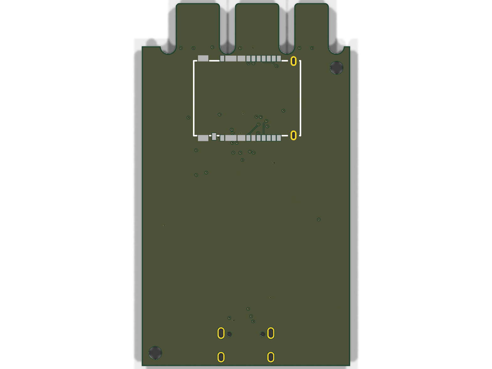
An RP2040 board shaped to fit a PlayStation memory-card shell, with native USB-C and push-push microSD storage. It targets the open-source PicoMemcard firmware pinout and was designed end-to-end in Fabdesk.
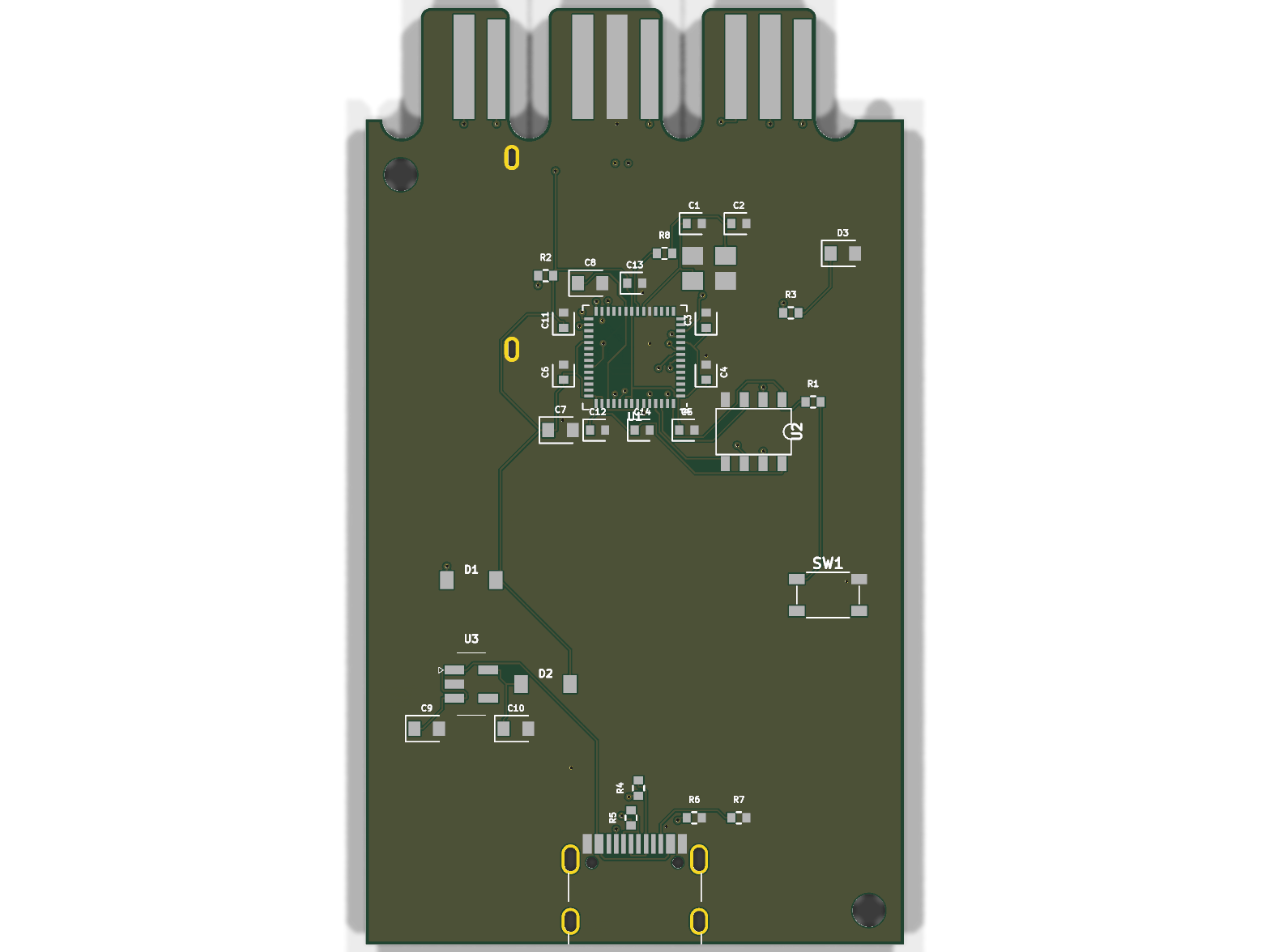
Prototype status: the PCB is fully routed and passes KiCad PCB DRC with zero errors and zero unconnected items. It has not yet been manufactured or bench-tested. Review the design and prototype cautiously before connecting it to a console.
| Function | RP2040 GPIO |
|---|---|
| PS1 DAT | GP5 |
| PS1 CMD | GP6 |
| PS1 SEL | GP7 |
| PS1 CLK | GP8 |
| PS1 ACK | GP9 |
| microSD DAT0/MISO | GP16 |
| microSD CD/DAT3/CS | GP17 |
| microSD CLK | GP18 |
| microSD CMD/MOSI | GP19 |
| Status LED | GP25 |
circuit.tsx — authoritative Fabdesk/tscircuit sourceoutline.ts — PS1 memory-card board outline derived from PicoMemcardfabdesk.json — four-layer routing and manufacturing constraintsboard.kicad_pcb, board.kicad_sch, board.kicad_pro — generated KiCad project; the PCB is the final routed boardboard.dsn, board-final.ses — final Specctra routing exchange filesrenders/ — top and bottom board rendersreports/final-drc.json — KiCad 10 DRC resultexports/gerbers/ — Gerbers and Excellon drill outputexports/bom.csv, exports/positions.csv — cleaned BOM and pick-and-place dataexports/fabrication.zip — ready-to-review fabrication bundleOpen this directory as a Fabdesk project and build circuit.tsx. The committed board.kicad_pcb contains the final FreeRouting route and GND fills. Regenerating KiCad from circuit.json will recreate an unrouted board, so keep or branch the committed PCB before converting again.
Manufacturing constraints used for the final board:
| Constraint | Value |
|---|---|
| Copper layers | 4 |
| Board thickness | 1.6 mm |
| Minimum trace width | 0.10 mm |
| Minimum clearance | 0.10 mm |
| Via diameter / drill | 0.45 / 0.20 mm |
| Minimum copper-to-edge | 0.20 mm |
The final PCB reports 465 routed track segments, 43 vias, zero DRC errors, and zero unconnected items. The remaining DRC notices are cosmetic generated-footprint silkscreen/text warnings. Fabdesk's current circuit-json-to-KiCad converter emits incorrect metadata for some custom schematic symbols, so KiCad ERC output is not used as the release gate; circuit.tsx, the PCB netlist, and PCB DRC are authoritative.
exports/fabrication.zip is a reviewable starting package, not a substitute for your fabricator's upload preview and rule check.The mechanical outline and console-contact placement are derived from dangiu/PicoMemcard, licensed under GPL-3.0. The RP2040 support circuit follows Raspberry Pi's Hardware design with RP2040.
This repository is licensed under the GNU General Public License v3.0. See LICENSE.
PlayStation is a trademark of Sony Interactive Entertainment. This is an independent open-hardware project and is not affiliated with or endorsed by Sony.
| Qty | Value | Footprint | References |
|---|---|---|---|
| 8 | tscircuit:chip | J1_ACK, J1_CLK, J1_CMD, J1_DAT, J1_GND, J1_NC, J1_SEL, J1_VCC | |
| 8 | 100nF | tscircuit:capacitor_cap0402 | C3, C4, C5, C6, C11, C12, C13, C14 |
| 4 | 1uF | tscircuit:capacitor_cap0603 | C7, C8, C9, C10 |
| 3 | 1kΩ | tscircuit:resistor_res0402 | R1, R3, R8 |
| 2 | tscircuit:hole_circle_holeDiameter2.2mm | , | |
| 2 | 15pF | tscircuit:capacitor_cap0402 | C1, C2 |
| 2 | 27Ω | tscircuit:resistor_res0402 | R4, R5 |
| 2 | 5.1kΩ | tscircuit:resistor_res0402 | R6, R7 |
| 2 | D | tscircuit:SS14 | D1, D2 |
| 1 | 10kΩ | tscircuit:resistor_res0402 | R2 |
| 1 | ABM8-272-T3 | tscircuit:ABM8-272-T3 | Y1 |
| 1 | AP2112K-3.3TRG1 | tscircuit:AP2112K-3_3TRG1 | U3 |
| 1 | CS-204 | tscircuit:CS-204 | J3 |
| 1 | LED | tscircuit:led_0603_color_green | D3 |
| 1 | RP2040 | tscircuit:RP2040 | U1 |
| 1 | SW1 | tscircuit:push_button_smdpushbutton | SW1 |
| 1 | TYPE-C-31-M-12 | tscircuit:TYPE-C-31-M-12 | J2 |
| 1 | W25Q16JVSSIQ | tscircuit:W25Q16JVSSIQ | U2 |
FujiNetWIFI/fujinet-hardware
Schematics and design files for FujiNet hardware

mrcha033/hw-codesign
Agentic hardware co-design: brief to KiCad, firmware, 3D review, and explicit fabrication blockers.

TechnikWeber/convertible-keyboard-pcb
Convertible keyboard PCB: full-size ISO-DE & ANSI with a snap-off numpad that turns it into a TKL (RP2040, USB-C, KiCad). Cheap, clean, modern core to build on — looking for a case designer.

C-yue28/Plant-Monitor
ML-powered plant monitor, tracking metrics such as temperature, humidity, soil moisture, etc to inform plant watering behavior.


FugLong/OpenChord
An open-source music device for portable, expressive, and extensible audio creation.


enkhbold470/kicad-projects
Five KiCad 10 boards (4- and 6-layer): ESP32-S3 industrial gateway, USB-C PD bench supply, RP2040 logic analyzer, FOC motor controller, iCE40 FPGA board.
It measures 36.2 × 63.1 mm and has 4 copper layers, 1.6 mm thick.
42 parts, built around the RP2040, W25Q16JVSSIQ, CS-204 and AP2112K-3.3TRG1. The full list of its parts is on this page, with links to each part's symbol and footprint where PCBKit's library has them.
From the fabPlane/ps1-memory-card-usb repository on GitHub, at the commit this page was made from: the board is board.kicad_pcb and its schematic board.kicad_sch. PCBKit opens the board in the browser, with nothing to install.
Its repository publishes it under the GPL-3.0 licence: you may reuse it on that licence's terms (keep the author's notice, and for a copyleft licence share your changes alike).