6 layers300 × 248.8 mm

 fabPlane/gb-devcart
A simple, original Game Boy (DMG) / ModRetro Chromatic homebrew development cartridge. 512 KB of rewritable NOR flash, 8 KB of battery-free F-RAM, and an MBC5-subset mapper built from discrete 74HC logic.
Gb devcart is an open-source printed circuit board by fabPlane, from the fabPlane/gb-devcart repository on GitHub. It is a 2-layer board of 56 × 49.5 mm with 26 parts on 52 nets, routed with 868 tracks and 118 vias.
It is built around the SST39SF040-55-4I-NHE-T, SN74HC32DR(LX) and SN74HC00DR(LX), with the 74HC574D, FM18W08-SGTR and CC0603KRX7R9BB104 among its other parts. Its parts include 7 capacitors, 6 resistors, 6 ICs and 1 connector.


A simple, original Game Boy (DMG) / ModRetro Chromatic homebrew development cartridge. 512 KB of rewritable NOR flash, 8 KB of battery-free F-RAM, and an MBC5-subset mapper built from discrete 74HC logic. 2-layer, 56 x 49.5 mm, 32 edge fingers at 1.5 mm pitch, 5 V bus.
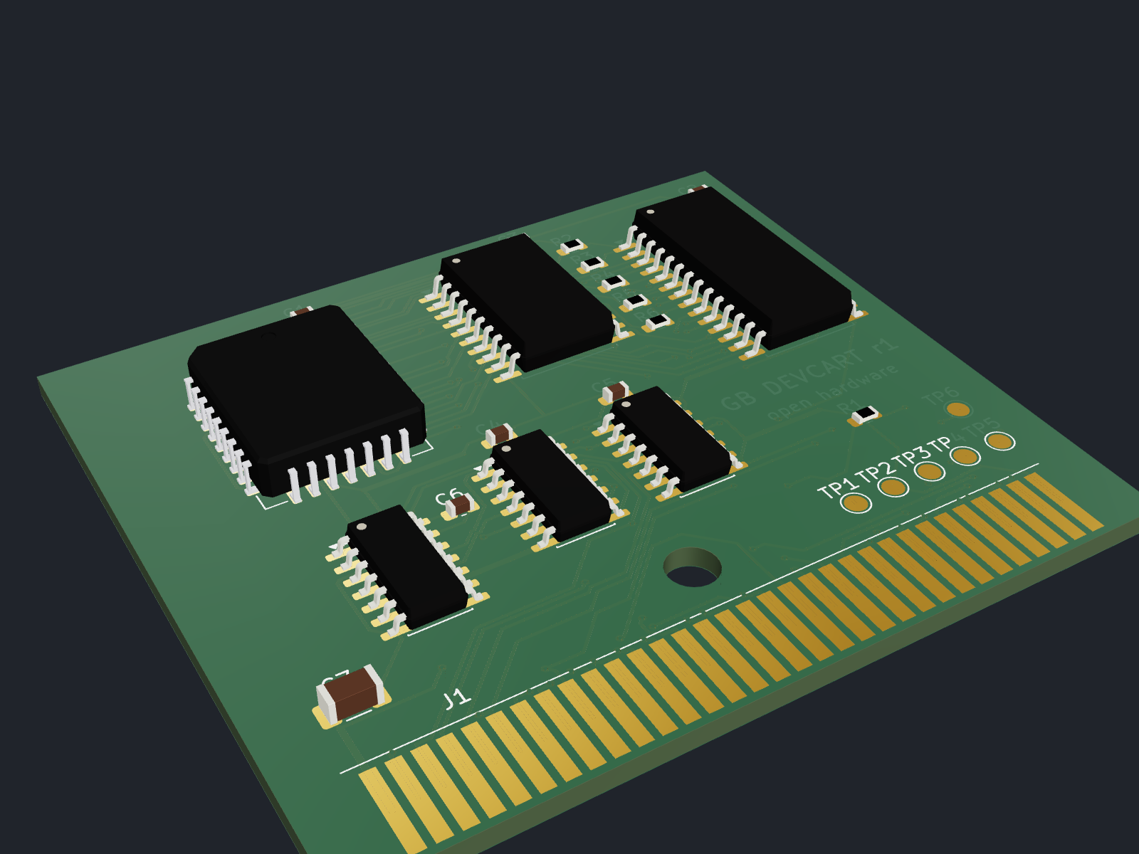
Status: fully routed (2 layers, Freerouting through fabdesk), DRC/ERC clean, in-stock JLCPCB parts with LCSC numbers, JLC gerbers/BOM/CPL in
exports/jlcpcb/. Not yet built or tested on hardware.
Designed with fabPlane (fabdesk) driving Claude Code. Inspired by the ModRetro "Demo Cartridge", but an original, much simpler design: no FPGA, no level shifters, no regulators.
| What | Where |
|---|---|
| KiCad project (schematic, board, custom symbols/footprint) | board.kicad_*, lib/, circuit.netlist.json |
| 3D models of every part, 3D renders, STEP of the whole board | 3dmodels/, renders/, exports/board.step |
| USB programmer (Arduino Mega firmware + PC tool + cart simulator) | programmer/ |
| Demo homebrew game "Bit Catcher" (GBDK-2020) | game/ |
| JLCPCB / LCSC price list | docs/jlcpcb-pricing.md |
# build the demo game (GBDK-2020)
make -C game GBDK_HOME=/path/to/gbdk
# test the programmer end to end against the cart simulator (no hardware needed)
programmer/test_e2e.sh
# flash a real cart through an Arduino Mega 2560 (see programmer/README.md for wiring)
python3 programmer/host/gbflash.py --port /dev/ttyACM0 flash game/dist/bitcatcher.gb| Top | Bit Catcher on the cart |
|---|---|
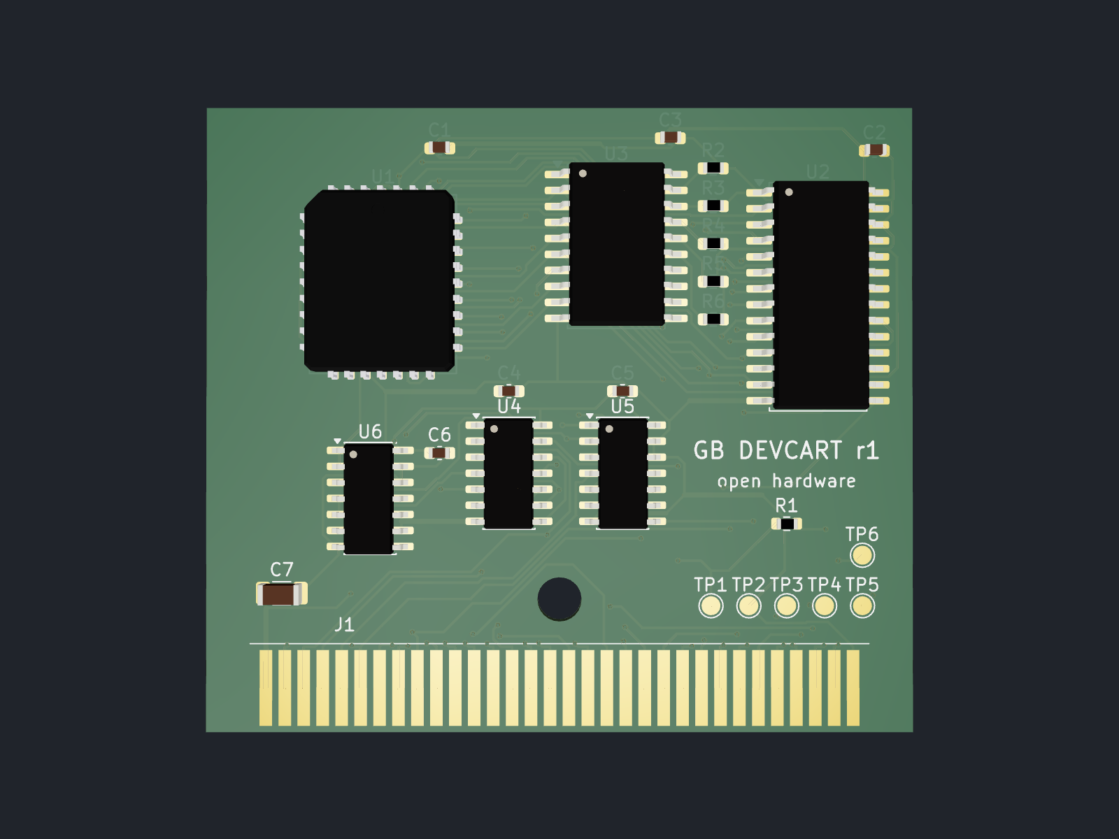 | 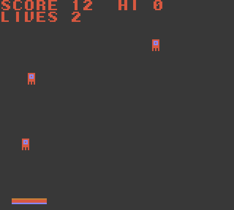 |
| GB address | Access | Function |
|---|---|---|
| 0x0000–0x3FFF | R | ROM bank 0 (fixed): flash 0x00000–0x03FFF |
| 0x4000–0x7FFF | R/W | ROM bank N (switchable): flash N*0x4000 + (addr & 0x3FFF), N = 0–31 |
| 0x2000–0x2FFF | W | Bank register (74HC574, bits 0–4 used, bits 5–7 latched but unconnected) |
| 0xA000–0xBFFF | R/W | 8 KB F-RAM (FM18W08, A13/A14 tied low), always enabled |
Notes:
| Signal | Equation |
|---|---|
| Flash /CE | A15 |
| Flash /OE, FRAM /OE | /RD |
| Flash /WE | `/WR |
| Latch clock (rising edge latches) | `/WR |
| Latch /OE | /A14; outputs are pulled down (2.2 kΩ), so A14=0 gives bank 0 |
| FRAM /CE | `/CS |
| FRAM /WE | /WR |
The flash sees A0–A13 from the bus and A14–A18 from the latch (D0–D4).
Run the flasher from WRAM/HRAM, because the flash returns status instead of data while busy. Interrupts off. All command cycles go through the switchable window, so bank-register writes at 0x2000 never reach the flash.
The SST39SF040 decodes commands on address bits A14–A0 only: 0x5555 and 0x2AAA.
0x5555 needs chip A14 = 1, so select an odd bank (e.g. 1) and write to GB 0x5555.0x2AAA needs chip A14 = 0, so select an even bank (e.g. 0) and write to GB 0x6AAA.Byte program of data to chip address X:
[0x2000]=1; [0x5555]=0xAA[0x2000]=0; [0x6AAA]=0x55[0x2000]=1; [0x5555]=0xA0[0x2000]=X>>14; [0x4000 + (X & 0x3FFF)]=dataSector erase (4 KB) at SA: the same first two cycles, then [0x2000]=1; [0x5555]=0x80,
[0x5555]=0xAA, [0x2000]=0; [0x6AAA]=0x55, then [0x2000]=SA>>14; [0x4000+(SA&0x3FFF)]=0x30.
Chip erase: the same, with the last cycle [0x2000]=1; [0x5555]=0x10. Then poll as above.
Program a 16 KB bank only from a bank other than the one being written, or from RAM, and verify by read-back. Keep bank 0 (vectors, header, flasher stub) write-protected by software convention.
/RESET has a 10 kΩ pull-up (R1). AUDIO_IN is unconnected except for test pad TP6./CS decode assumes /CS is asserted for A15 = 1; verify on the target hardware.| Ref | Qty | Value | Package | Suggested MPN |
|---|---|---|---|---|
| U1 | 1 | 512 KB 5 V NOR flash | PLCC-32 | SST39SF040-70-4C-NHE |
| U2 | 1 | 32 KB F-RAM | SOIC-28W | FM18W08-SG |
| U3 | 1 | 74HC574 | SOIC-20W | SN74HC574DWR |
| U4, U5 | 2 | 74HC32 | SOIC-14 | SN74HC32DR |
| U6 | 1 | 74HC00 | SOIC-14 | SN74HC00DR |
| C1–C6 | 6 | 100 nF X7R | 0603 | — |
| C7 | 1 | 10 µF X5R | 1206 | — |
| R1 | 1 | 10 kΩ | 0603 | — |
| R2–R6 | 5 | 2.2 kΩ | 0603 | — |
| TP1–TP6 | 6 | test pad D1.5 mm | — | — |
| J1 | 1 | edge fingers (PCB feature) | gbdev:GB_Cart_Edge_32 | — |
The cart is programmed by an Arduino Mega 2560 (5 V I/O, so no level shifters) wired to a
32-pin Game Boy cartridge slot. The PC runs programmer/host/gbflash.py
(info, flash, dump, erase, save-backup, save-restore). The flashing algorithm lives in
programmer/firmware/gbflash/gbflash_core.h, which also compiles into a native simulator of this
cart for hardware-free tests. See programmer/README.md for the wiring table.
Every component carries a 3D model, vendored in 3dmodels/ and referenced as
${KIPRJMOD}/3dmodels/…, so the project renders and exports (STEP/GLB) with no global KiCad
3D library. The passives and SOIC models come from the official KiCad 3D library
(CC-BY-SA 4.0 with the KiCad library exception). KiCad ships no PLCC-32 model, so
scripts/make_plcc32_model.py generates one with CadQuery (JEDEC MS-016 body, 32 J-leads)
matching the KiCad footprint. Regenerate the renders with:
kicad-cli pcb export glb --include-pads --include-silkscreen --include-soldermask -o renders/board.glb board.kicad_pcb
kicad-cli pcb export step -o exports/board.step board.kicad_pcb
cd scripts/render3d && npm install && CHROMIUM_PATH=/path/to/chrome npm run render # -> renders/3d-*.pngSee docs/jlcpcb-pricing.md for bare-PCB and assembled prices at
JLCPCB with LCSC part numbers. Order ENIG (or hard-gold fingers with a 45° bevel) and 1.0 mm
thickness so the board fits a standard DMG cartridge shell.
JLC order files (regenerate with KICAD_CLI=… python3 scripts/jlc_export.py):
| File | Upload as |
|---|---|
exports/jlcpcb/gerbers.zip | Gerber files (2 layers, 56 × 49.5 mm) |
exports/jlcpcb/bom.csv | Assembly BOM: 9 lines, every line with an LCSC part number |
exports/jlcpcb/cpl.csv | Assembly pick-and-place (19 parts, top side) |
Check the rotation preview on JLC's assembly page before confirming. SOIC and PLCC reels sometimes need a ±90° correction.
| Routed top (F.Cu) | Routed bottom (B.Cu) |
|---|---|
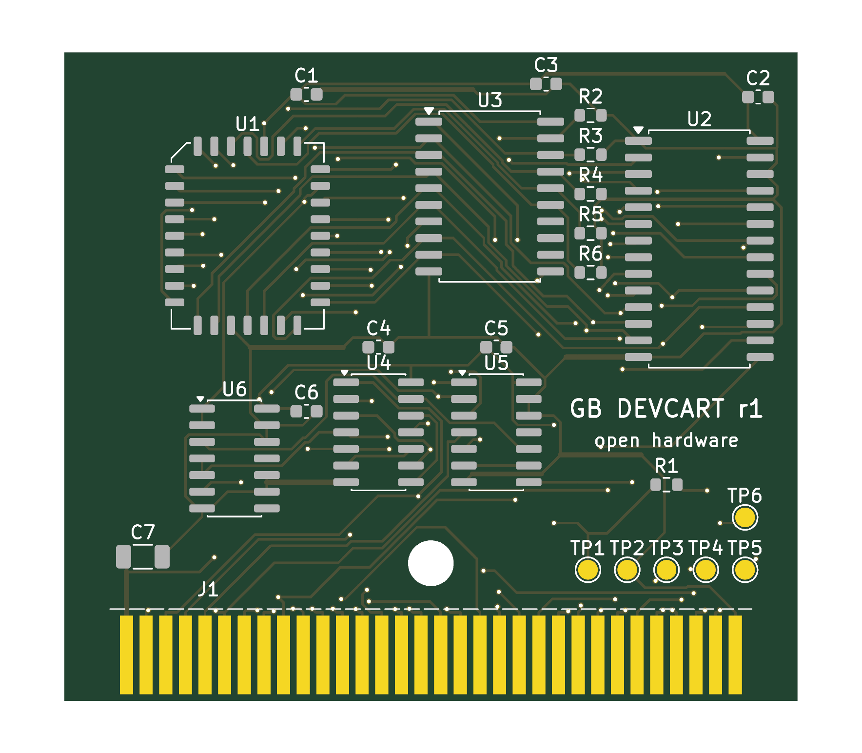 | 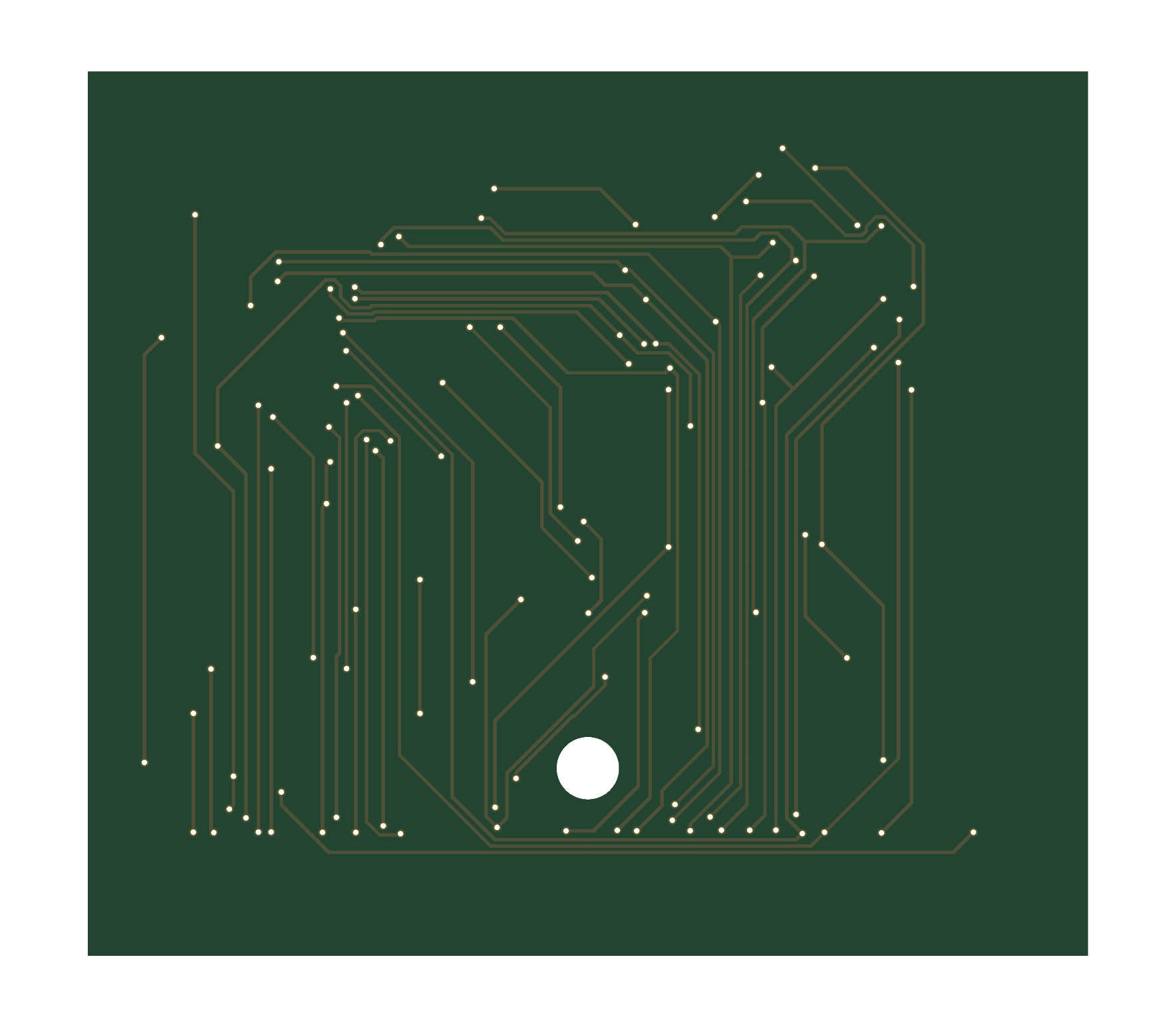 |
Snapshot from 2026-10-01 (USD, before shipping):
| Qty | Bare PCB, ENIG | PCB + Economic assembly |
|---|---|---|
| 5 | $18.60 ($3.72/board) | |
| 10 | $21.60 ($2.16/board) | |
| 30 | $28.90 ($0.96/board) | |
| 100 | $62.70 ($0.63/board) |
Before ordering:
scripts/sync_fields.py copies MPN / Manufacturer / LCSC from the netlist into board.kicad_pcb and board.kicad_sch.scripts/jlc_export.py writes the JLC gerbers, BOM and CPL.scripts/gen.py generates lib/gbdev.kicad_sym, lib/gbdev.pretty/ and circuit.netlist.json. The netlist is the source of truth; board.kicad_* are built from it.gbdev library) because the build environment has no KiCad symbol libraries.gbdev symbols and edge footprint; placement inside the 56 x 49.5 mm
outline, with all parts above y = 41.5 mm and the 3.5 mm boss hole at (28, 39).route_run. All 134 connections are routed
in one run.
capacity router (fab_router) could not route this dense
2-layer bus. Its best result was 63 of 134 connections, and long runs block the bridge process until
fabdesk times out. To get to the result above, parts were moved (U2, U3, C2, C3, C6, R2–R6), the rules
were tightened as listed, and Freerouting was enabled.board.kicad_pcb by hand.
A circuit_build with fresh: true will discard them, along with the routing./CS decode assumption,
and the JLC rotation offsets.| Qty | Value | Footprint | References |
|---|---|---|---|
| 6 | 100nF | Capacitor_SMD:C_0603_1608Metric | C1, C2, C3, C4, C5, C6 |
| 5 | 2.2k | Resistor_SMD:R_0603_1608Metric | R2, R3, R4, R5, R6 |
| 2 | 74HC32 | Package_SO:SOIC-14_3.9x8.7mm_P1.27mm | U4, U5 |
| 1 | 10k | Resistor_SMD:R_0603_1608Metric | R1 |
| 1 | 10uF | Capacitor_SMD:C_1206_3216Metric | C7 |
| 1 | 74HC00 | Package_SO:SOIC-14_3.9x8.7mm_P1.27mm | U6 |
| 1 | 74HC574 | Package_SO:SOIC-20W_7.5x12.8mm_P1.27mm | U3 |
| 1 | FM18W08 | Package_SO:SOIC-28W_7.5x17.9mm_P1.27mm | U2 |
| 1 | GB_Cart_Edge_32 | gbdev:GB_Cart_Edge_32 | J1 |
| 1 | SST39SF040 | Package_LCC:PLCC-32_11.4x14.0mm_P1.27mm | U1 |
| 1 | TP_AUDIO_IN | TestPoint:TestPoint_Pad_D1.5mm | TP6 |
| 1 | TP_CLK | TestPoint:TestPoint_Pad_D1.5mm | TP3 |
| 1 | TP_GND | TestPoint:TestPoint_Pad_D1.5mm | TP2 |
| 1 | TP_RD | TestPoint:TestPoint_Pad_D1.5mm | TP5 |
| 1 | TP_VCC | TestPoint:TestPoint_Pad_D1.5mm | TP1 |
| 1 | TP_WR | TestPoint:TestPoint_Pad_D1.5mm | TP4 |
It measures 56 × 49.5 mm and has 2 copper layers, 1.6 mm thick.
26 parts, built around the SST39SF040-55-4I-NHE-T, SN74HC32DR(LX), SN74HC00DR(LX) and 74HC574D. The full list of its parts is on this page, with links to each part's symbol and footprint where PCBKit's library has them.
From the fabPlane/gb-devcart repository on GitHub, at the commit this page was made from: the board is board.kicad_pcb and its schematic board.kicad_sch. PCBKit opens the board in the browser, with nothing to install.
Its repository states no licence, so its author keeps all rights: ask fabPlane before reusing the design.


nanamitm/td4-kicad
TD4 4-bit CPU (from the book CPUの創りかた) as a KiCad 10 hierarchical schematic

nfbeier/HusseinLab_UltrafastPlasmaScience
Github repository for hardware and software interfacing of the smart system used by the Hussein Ultrafast Plasma Science group at the University of Alberta for experiments LIBS and high-repetition-rate, femtosecond…


Takazudo/zudo-osc-hole-field
This directory retains the rejected #38 nine-board-era schematic, PCB and route receipts at base commit 1fc6e5347308fe5e8166d5828ba3ba6fa8e101c7. It is excluded from the current ten-board manifest.

AzonInc/Doorman
ESP32-S3 based Intercom Gateway (TCS / Koch / Niko / Scantron / Analogue Systems)