2 layers116 × 102 mm

 eutectic6337/coin13
a challenge coin with blinky lights
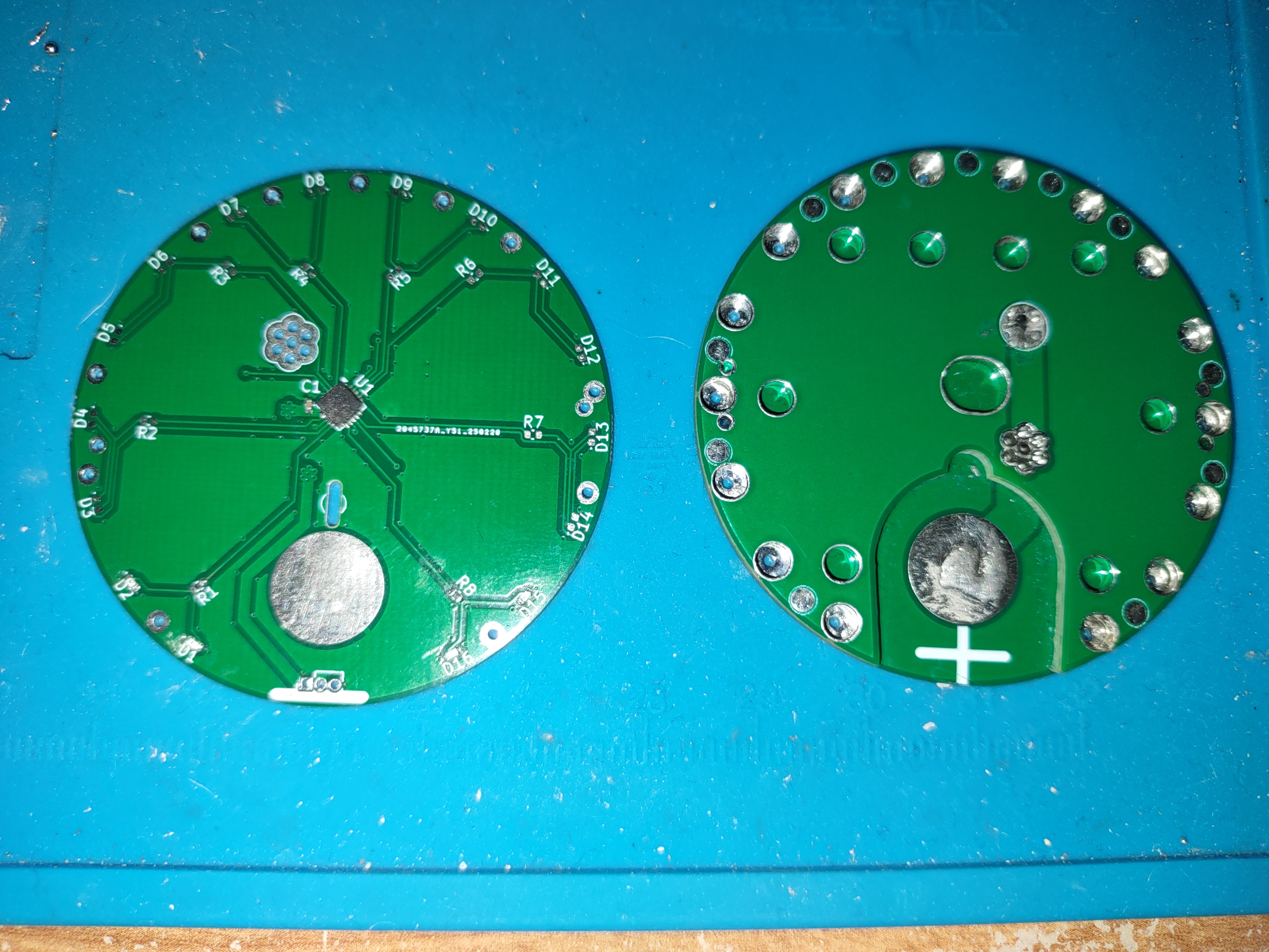
Internal is an open-source printed circuit board by eutectic6337, from the eutectic6337/coin1 repository on GitHub, published under the CC0-1.0 licence. It is a 2-layer board of 50 × 48.6 mm with 48 parts on 2 nets, routed with 6 tracks and 0 vias.
challenge coin with blinky lights
Feature: Using 8 PWM channels to provide dimming function for 16 LEDs by connecting pairs in anti-parallel between a PWM pin and a GPIO.
built as a stack of 3 PCBs - components mounted on top of bottom board, second board has a cutout to fit a battery and for each mounted component, and top board has holes to transmit light from LEDs
finished coin to have [relatively] smooth top and bottom
using JLCPCB's serial-number mechanism to put a unique number on each coin
Initial code flashed onto these is a modified version of the Arduino Blink demo.
| Qty | Value | Footprint | References |
|---|---|---|---|
| 25 | TestPoint_THTPad_3.0x3.0mm_Drill1.5mm | TestPoint:TestPoint_THTPad_3.0x3.0mm_Drill1.5mm | clearance-D1, clearance-D2, clearance-D3, clearance-D4, clearance-D5, clearance-D6, clearance-D7, clearance-D8, clearance-D9, clearance-D10, clearance-D11, clearance-D12, clearance-D13, clearance-D14, clearance-D15, clearance-D16 +9 |
| 11 | TestPoint_Pad_D2.0mm | TestPoint:TestPoint_Pad_D2.0mm | stitch2, stitch2, stitch2, stitch2, stitch2, stitch2, stitch2, stitch2, stitch2, stitch2, stitch2 |
| 7 | TestPoint_THTPad_D2.0mm_Drill1.0mm | TestPoint:TestPoint_THTPad_D2.0mm_Drill1.0mm | through-i1, through-i2, through-i3, through-i4, through-i5, through-i6, through-i7 |
| 4 | align-i1, align-i2, align-i3, align-i4 | ||
| 1 | TestPoint_Pad_D4.0mm | TestPoint:TestPoint_Pad_D4.0mm | contact-i1 |


hackclub/OnBoard
💡 Join 1,000 teenagers and make your first PCB with a $100 grant!

adamws/kicad-kbplacer
KiCad plugin for automatic keyboard's key placement and routing


softerhardware/Hermes-Lite2
A second generation low-cost amateur HF software defined radio transceiver.

CRImier/MyKiCad
My KiCad boards. Can't be bothered uploading individually anymore, so here you go.

loxodes/vna
Under development open hardware microwave vector network analyzer

fellesverkstedet/fabricatable-machines
Motion systems for flexible digital fabrication and research. Easy to fabricate and customize. Documentation: https://github.com/fellesverkstedet/fabricatable-machines/wiki
It measures 50 × 48.6 mm and has 2 copper layers, 1.6 mm thick.
48 parts. The full list of its parts is on this page, with links to each part's symbol and footprint where PCBKit's library has them.
From the eutectic6337/coin1 repository on GitHub, at the commit this page was made from: the board is hardware/internal/internal.kicad_pcb and its schematic hardware/smd0201/smd0201.kicad_sch. PCBKit opens the board in the browser, with nothing to install.
Its repository publishes it under the CC0-1.0 licence: you may reuse it on that licence's terms (keep the author's notice, and for a copyleft licence share your changes alike).