2 layers16.5 × 6.6 mm
Athan prog
et7ad/esp32_athan
A 16.5 × 6.6 mm board for flashing the clock without soldering a header onto J6. It carries two ordinary 2.54 mm male headers, one row apart:
2 partsMIT

 et7ad/esp32_athan
A 16.5 × 6.6 mm board for flashing the clock without soldering a header onto J6. It carries two ordinary 2.54 mm male headers, one row apart:
Esp32 athan is an open-source printed circuit board by et7ad, from the et7ad/esp32_athan repository on GitHub, published under the MIT licence. It is a 2-layer board of 59.6 × 50 mm with 39 parts on 54 nets, routed with 374 tracks and 121 vias.
It is built around the ESP32-S3-WROOM-1-N16R8 and AMS1117-3.3. Its parts include 10 resistors, 7 capacitors, 5 connectors, 4 ICs and 1 diode. It belongs with the ESP32 boards of this library.


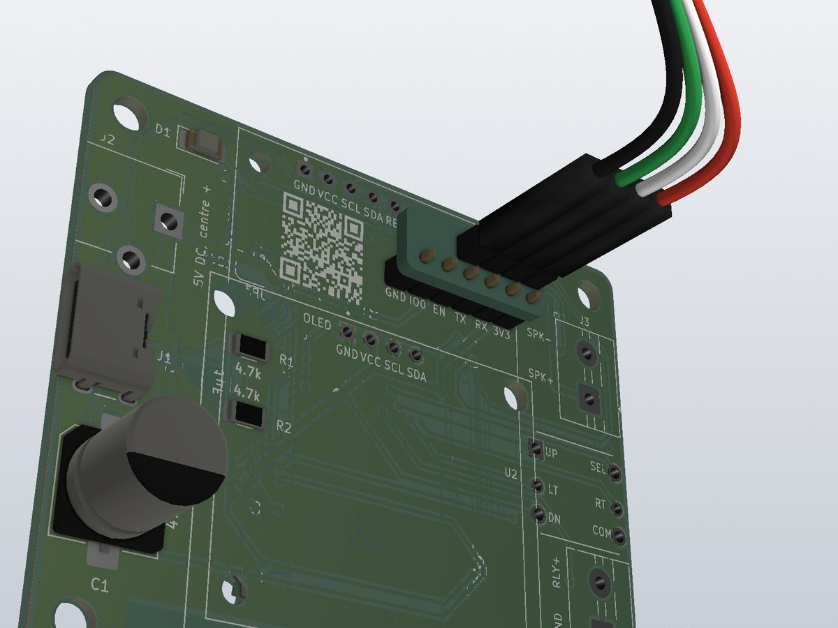
A 16.5 × 6.6 mm board for flashing the clock without soldering a header onto J6. It carries two ordinary 2.54 mm male headers, one row apart:
On the board, GPIO0 (IO0) is joined to GND, so the ESP32 starts in download mode as soon as it is powered through the programmer.
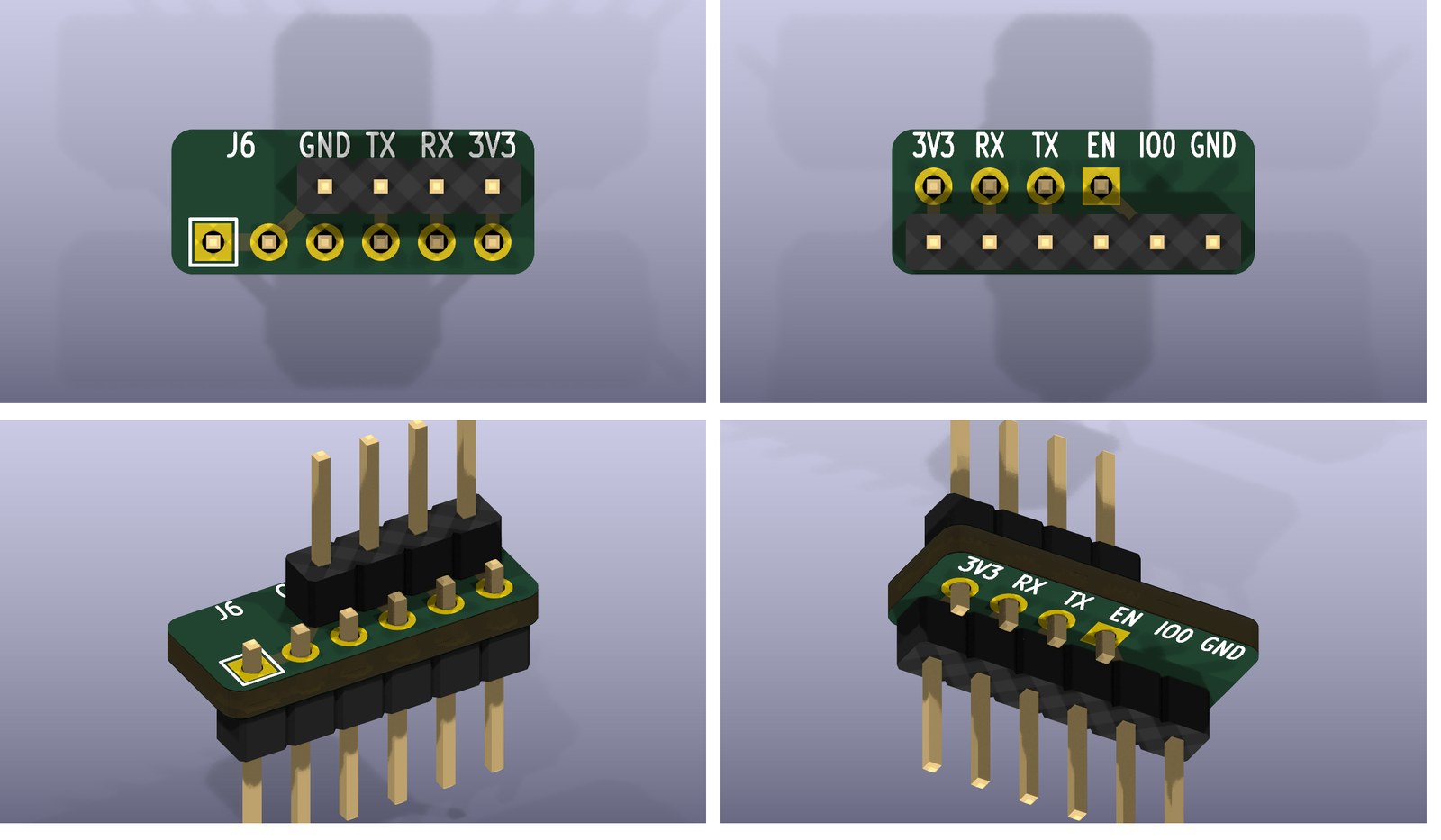
The top names the four jumper pins. The back names J6's six pins, each above the column of the J1 pin that goes into it (from the back, GND is at the right).
./generate_fab_files.sh (KiCad need not be open) writes fab_files/athan_prog.zip. Order it as a
2-layer board, 1.6 mm thick. The KiCad project is athan_prog.kicad_pro.| J1 pin (into J6) | J6 | Joined to |
|---|---|---|
| 1 | GND | J2 pin 1, GND |
| 2 | IO0 (GPIO0) | GND, on the board |
| 3 | EN | nothing (below) |
| 4 | TX (the ESP32's TXD0) | J2 pin 2, TX |
| 5 | RX (the ESP32's RXD0) | J2 pin 3, RX |
| 6 | 3V3 | J2 pin 4, 3V3 |
J2 sits over J1's pins 3 to 6. The ESP32 reads GPIO0 as it comes out of reset, and low means download mode. Whenever the programmer is out, the clock's own 4.7 kΩ pull-up (R4) keeps GPIO0 high.
Why EN is not connected. EN is the ESP32's reset, and the clock already drives it: R3 (4.7 kΩ to 3V3) and C5 (1 µF to GND) hold the ESP32 in reset for a few milliseconds after power comes on, then let it start. That start is when GPIO0 is read, and the programmer has already pulled GPIO0 low. Wiring EN to GND would hold the ESP32 in reset, and wiring it to 3V3 adds nothing to R3, so the pin only steadies the programmer in J6. Adapters that reset the chip by themselves use their DTR and RTS lines with two transistors; the programmer leaves that out to keep four wires. To start over in download mode, power the clock off and on again.
| Qty | Value | Footprint | References |
|---|---|---|---|
| 7 | 4.7k | Resistor_SMD:R_1206_3216Metric | R1, R2, R3, R4, R5, R8, R9 |
| 4 | MountingHole | MountingHole:MountingHole_3.2mm_M3 | H1, H2, H3, H4 |
| 3 | 22µF | Capacitor_SMD:C_1206_3216Metric | C2, C3, C6 |
| 3 | SolderJumper_2_Bridged | Jumper:SolderJumper-2_P1.3mm_Bridged_RoundedPad1.0x1.5mm | JP1, JP2, JP4 |
| 2 | 100nF | Capacitor_SMD:C_1206_3216Metric | C4, C7 |
| 1 | (100) | Resistor_SMD:R_1206_3216Metric | R11 |
| 1 | (100k) | Resistor_SMD:R_1206_3216Metric | R7 |
| 1 | 100 | Resistor_SMD:R_1206_3216Metric | R10 |
| 1 | 1µF | Capacitor_SMD:C_1206_3216Metric | C5 |
| 1 | 470µF | Capacitor_SMD:CP_Elec_8x10.5 | C1 |
| 1 | 5-way switch (SKQUCAA010 type) | SKQUAAA010:SKQUAAA010 | U2 |
| 1 | AMS1117-3.3 | Package_TO_SOT_SMD:SOT-223-3_TabPin2 | U3 |
| 1 | Barrel_Jack | Connector_BarrelJack:BarrelJack_CUI_PJ-102AH_Horizontal | J2 |
| 1 | ESP32-S3-WROOM-1-N16R8 | RF_Module:ESP32-S3-WROOM-1 | U1 |
| 1 | LED | LED_SMD:LED_1206_3216Metric_Pad1.42x1.75mm_HandSolder | D1 |
| 1 | MAX98357A | Package_DFN_QFN:TQFN-16-1EP_3x3mm_P0.5mm_EP1.23x1.23mm | U4 |
| 1 | OLED | Library:LCD_OLED_128X64_1.3_I2C | DS1 |
| 1 | PROG | Connector_PinHeader_2.54mm:PinHeader_1x06_P2.54mm_Vertical | J6 |
| 1 | Relay | TerminalBlock:TerminalBlock_MaiXu_MX126-5.0-02P_1x02_P5.00mm | J5 |
| 1 | SolderJumper_3_Open | Jumper:SolderJumper-3_P1.3mm_Open_RoundedPad1.0x1.5mm | JP3 |
| 1 | Speaker | TerminalBlock:TerminalBlock_MaiXu_MX126-5.0-02P_1x02_P5.00mm | J3 |
| 1 | TFT | Library:Display_TFT_1.54in_ST7789_240x240_8pin | DS2 |
| 1 | USB_C_Receptacle_PowerOnly_6P | Library:USB_C_Receptacle_GCT_USB4125_6P_BothSides | J1 |
| 1 | qrcode_back | Library:QRCode_esp32_athan_p3 | SYM2 |
| 1 | qrcode_front | Library:QRCode_esp32_athan_p3 | SYM1 |
et7ad/esp32_athan
A 16.5 × 6.6 mm board for flashing the clock without soldering a header onto J6. It carries two ordinary 2.54 mm male headers, one row apart:

NuttyShell/NuttyBadge
NuttyBadge: A NuttyShell crafted multi-tool. Opensourced Hardawre and Software

ajisrawi/dronemagnav
Magnetic-anomaly navigation (MagNav) board + firmware for drones: ESP32-S3, BMI088, LIS3MDL, BMP280, u-blox GNSS, WDMAM map matching, particle filter, MAVLink, phone route planner. Proprietary - all rights reserved.


kaorii-ako/inSomnia
Adaptive, context-aware wake clock — wakes you while you're already stirring, stays quiet if you're already up. ESP32-S3 + thermal array.

Studented0/PCB-Business-Card
A PCB business card with a little twist (A display and ESP32 to connect to lanyard and display spotify music and NFC)

zhangshua1/PenguinBotV3
PenguinBot V3.0 — 桌面轮足机器人 | ESP32-S3 定制PCB | ICM-42688-P SPI | TOF防跌落 | 离线唤醒词 | 自动充电坞 | BLE App | ¥589 BOM

AfriOrbit/SDR-IOT-project
This project includes all work materials for the SDR and IOT communication systems.
It measures 59.6 × 50 mm and has 2 copper layers, 1.6 mm thick.
39 parts, built around the ESP32-S3-WROOM-1-N16R8 and AMS1117-3.3. The full list of its parts is on this page, with links to each part's symbol and footprint where PCBKit's library has them.
From the et7ad/esp32_athan repository on GitHub, at the commit this page was made from: the board is hardware/pcb/esp32_athan.kicad_pcb and its schematic hardware/pcb/esp32_athan.kicad_sch. PCBKit opens the board in the browser, with nothing to install.
Its repository publishes it under the MIT licence: you may reuse it on that licence's terms (keep the author's notice, and for a copyleft licence share your changes alike).