
2 layers90 × 60 mm

Tap live cabling for inspection and injection
Tap is an open-source printed circuit board by ervanalb, from the ervanalb/lens repository on GitHub. It is a 4-layer board of 80 × 80 mm with 59 parts on 73 nets, routed with 850 tracks and 123 vias.
It is built around the PIC16F1454-I/P, G6K-2F-RF DC5 and MMA8653FCR1. Its parts include 22 connectors, 13 ICs, 9 capacitors, 6 resistors and 2 diodes. It belongs with the PIC boards of this library.


lens stands for "live editing of network streams"
lens is a framework that allows you to tap live cabling for inspection and injection.
Watch the video of our presentation here!
Slides & whitepaper are available in the docs/ folder.
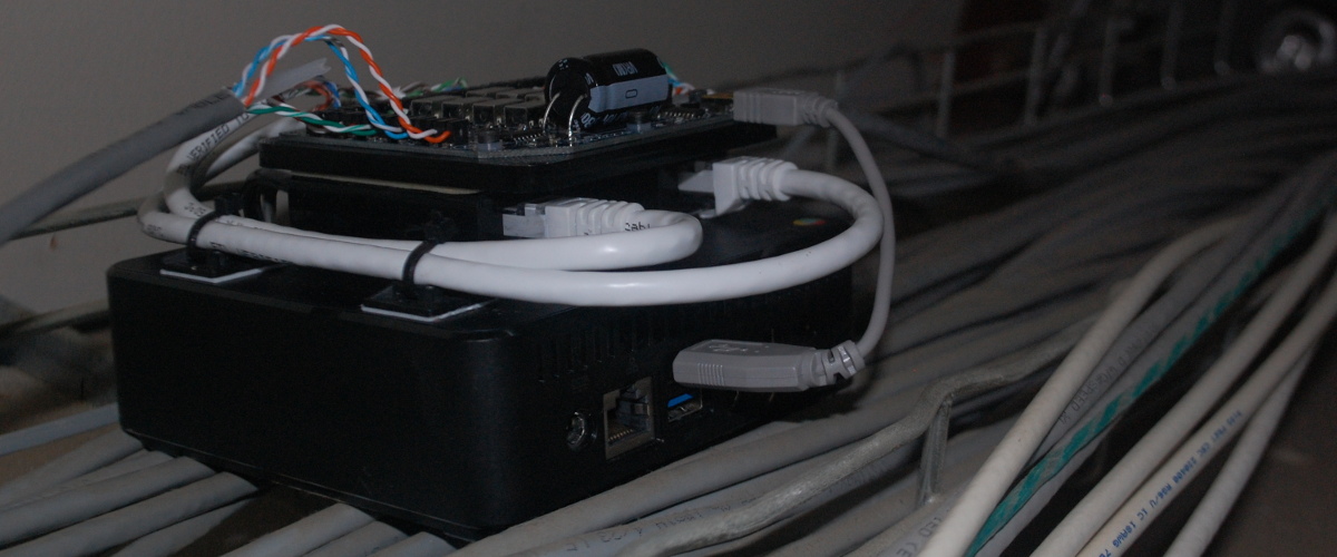
Or, photos of the device we presented can be found here.
You can reach us through github, or our emails are listed in our github profiles (Zach, Eric).
The wires of a network cable can be punched down into the lens tap board in two places without interrupting the packet flow. The tap board then provides a redundant copper path through a set of relays. Once all of the wires have been punched down on both sides, they can be cut so that the signals are now routed only through the relays on the tap board.
One or two additional NICs are connected to the tap board on its TAP ports. These, along with a USB link, are connected to a computer. The computer can command the relays over USB to assume either a passive or active tap topology, or a transparent pass-through mode.
The tap board has three safety features: fail-safe power loss, heartbeat, and tamper detection. If the board detects that power has been lost, it can optionally use the remaining energy stored in a large capacitor to revert the state of the relays to pass-through mode. Alternatively, if the board fails to receive a heartbeat from the computer within a specified amount of time, such as if the computer software crashes, it can revert the relays. Lastly, the board has an accelerometer on it that can detect if the board is jostled or moved and report that to the computer. This can give you peace of mind that your board is still in-place and working.
The lens software was made to work nicely with the tap board, but can be used without it. Simply connect two NICs in a man-in-the-middle configuration.
lens implements a software network stack designed for man-in-the-middle attacks. It is able to decode many protocols, edit their data payloads, and forge new packets containing the modified payloads that look as similar to the original ones as possible.
lens is single-threaded and uses asynchronous I/O through tornado. Many operations are implemented as tornado coroutines.
The software is split into layers, each of which manages its own state and provides an abstraction for the layers above it. These layers generally follow the standard "OSI Model." For instance, Ethernet, IPv4, TCP, HTTP, are some of the layers we have.
Some layers are inherently stateful with respect to the data that is passed through them (e.g. TCP), whereas others do not require any state to handle their data (e.g. IPv4). However, these layers may find it useful to maintain state in order to later forge packets.
Layers are represented as subclasses of NetLayer. Layers are chained together to form a doubly-linked DAG (typically a tree), where each layer knows its parent (parent) and its children (children) that come "above" it in the stack. For example, an instance of EthernetLayer may have an IPv4Layer in its children list. That IPv4Layer's parent would be a reference back to the EthernetLayer instance.
For the purposes of this document, this kind of relationship will be described as EthernetLayer --> IPv4Layer, even though the connection is in fact double-ended, and the layers are instances.
Each layer (subclassing NetLayer) should implement the following methods as tornado coroutines:
Layer.on_read(self, src, header, payload)This coroutine is called whenever there is new data (payload) available for the layer to process. header is a dict which holds all of the information extracted from all of the previous layers. With payload and header, it should be possible to completely reconstruct the original packet. src represents where the data came from. A simple on_read might move some data from payload into header and call Layer.bubble(src, new_header, sub_payload) to pass data to children layers.
Layer.write(self, dst, header, payload)This coroutine is called to write out payload. A simple write would take relevant parameters in header, re-serialize them, and combine them with payload to form a new payload. It would then call Layer.write_back(dst, header, new_payload) to pass the back to the parent layer.
Layer.match(self, src, header)This function should return a boolean indicating whether this layer is capable of handling the given packet. The default behavior, if not overridden, is to always return True, that is, consume all data.
Currently, src and dst parameters represent which physical NIC the message came from or is intended to go to. NetLayer implements two functions, route(src) and unroute(dst), which are intended to resolve the intended recipient of a packet. This mechanism might need to be re-worked for systems with 3+ NICs. Currently, the two NICs are represented by 0 and 1, so the functions are equivalent.
Although each NetLayer should implement the methods above, there are some additional helper methods/coroutines that are useful:
Layer.bubble(self, src, header, payload)This coroutine will attempt to further decode a payload using this layer's children. It will go through the list of children until it finds one whose match(...) function returns True. It will then call that child's on_read(...) function. If no child matches, it calls self.write(dst, ...), resolving dst from src, at which point the program flow "reverses direction".
This method is used to pass data on to higher layers for further decoding. If no higher layer is available or connected it will re-write (loopback) the data unchanged.
Layer.write_back(self, dst, header, payload)This coroutine calls self.parent.write(dst, header, payload). It is for further encoding a payload using this layer's parent. It can be thought of as the opposite of Layer.bubble(...).
Layer.passthru(self, src, header, payload)This convenience coroutine will call self.write_back(dst, ...) with dst resolved from src.
| Qty | Value | Footprint | References |
|---|---|---|---|
| 8 | G6K-2F-RF | G6K-2F-RF | U1, U2, U3, U4, U5, U6, U7, U8 |
| 6 | VAL** | HOLE | HOLE, HOLE, HOLE, HOLE, HOLE, HOLE |
| 5 | 100n | SM0603_Capa | C2, C6, C7, C8, C9 |
| 4 | CONN_1 | 1pin | P3, P8, P22, P23 |
| 4 | D | 00-9176-002 | P5, P10, P15, P20 |
| 4 | DTAP | 00-9176-002 | P4, P9, P14, P19 |
| 4 | H | 00-9176-002 | P1, P6, P11, P16 |
| 4 | HTAP | 00-9176-002 | P2, P7, P12, P17 |
| 2 | 10K | SM0603_Resistor | R2, R3 |
| 2 | 1u | SM0603_Capa | C4, C5 |
| 2 | 4K7 | SM0603_Resistor | R5, R6 |
| 2 | 74LS595 | SO16N | U11, U12 |
| 1 | 100R | SM0603_Resistor | R4 |
| 1 | 22R | SM0603_Resistor | R1 |
| 1 | 3v3 | SOT23 | U9 |
| 1 | 470nF | SM0603_Capa | C1 |
| 1 | 6800u 10V | C2V10 | C3 |
| 1 | DIODE | DO-214AC(SMA) | D1 |
| 1 | FERRITE | SM0603_Capa | L1 |
| 1 | ICSP | SIL-6 | P21 |
| 1 | LED | LED-0603 | D2 |
| 1 | MMA8653FC | DFN_10 | U13 |
| 1 | PIC16F1454 | SO14N | U10 |
| 1 | USB-MINI-B | USB_MINI_B | CON1 |
It measures 80 × 80 mm and has 4 copper layers, 1.6 mm thick.
59 parts, built around the PIC16F1454-I/P, G6K-2F-RF DC5 and MMA8653FCR1. The full list of its parts is on this page, with links to each part's symbol and footprint where PCBKit's library has them.
From the ervanalb/lens repository on GitHub, at the commit this page was made from: the board is hardware/tap.kicad_pcb. PCBKit opens the board in the browser, with nothing to install.
Its repository states no licence, so its author keeps all rights: ask ervanalb before reusing the design.


DiegoRosales/PCB_Designs
This repository contains some of the designs I've made. Everything here is Open Source Hardware

tdarlic/making-embedded-systems
Making Embedded Systems class - Elicia White


dolson14/k7arx
Circuit and PCB Designs, anything else related to radio and electronics