
2 layers85.4 × 54.1 mm

 Erox-02/NFC
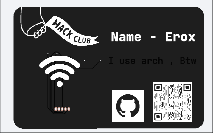
The integrated planar antenna harvests power from the phone's magnetic field to light up the led placed in front side pcb layer while simltaniously doing nfc connection with phone/other device .
NFC is an open-source printed circuit board by Erox-02, from the Erox-02/NFC repository on GitHub, published under the GPL-3.0 licence. It is a 2-layer board of 72.6 × 46.1 mm with 12 parts on 7 nets, routed with 98 tracks and 10 vias.
It is built around the NT3H2111W0FHKH. Its parts include 3 resistors, 1 IC, 1 diode, 1 connector and 1 inductor. It belongs with the radio and wireless boards of this library.
A basic nfc card with custom antenna .
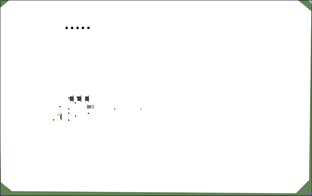
The integrated planar antenna harvests power from the phone's magnetic field to light up the led placed in front side pcb layer while simltaniously doing nfc connection with phone/other device . Also i have left some traces for later i2c uses .
Check out my project's build video's on forge
you can re use my antenna and add custom footprint for others , or you can swap my name and qr with your own :D .
I will use pcba on jlc pcb to order it because the parts are kinda rare in india and if i order frm lcsc , it will cost me more for shipping and moq .
But if you wanna solder/rework on your own , order the parts frm given links in bom and solder the components on the designated places as cpl.xlsx says , then connect the card with your nfc enabled phone and bind a url . Or you can use a esp 32/other mpu and rewrite the eeprom with i2c , **REMINDER : USE 2.2-3v POWER SUPPLY **
detailed steps for non pcba :
The antenna is supposed to harvest energy from the nfc field, which is more than enough to power the led while the nfc ic communicates with the phone or whatever nfc device youre using.
me , mineself Erox aka Dipanjan
| Designator | Comment | Footprint | Quantity | LCSC Part # | LCSC Link | Unit Price |
|---|---|---|---|---|---|---|
| Cap1 | 180 nf | Capacitor_SMD:C_0603_1608Metric | 1 | C519440 | https://www.lcsc.com/product-detail/C519440.html | $0.0114 |
| D1 | LED | LED_0603_1608Metric | 1 | C19171394 | https://www.lcsc.com/product-detail/C19171394.html | See LCSC |
| R1 | 5k ohm | Resistor_SMD:R_0603_1608Metric | 1 | C862232 | https://www.lcsc.com/product-detail/Chip-Resistor-Surface-Mount_YAGEO-RT0603BRE075KL_C862232.html | $0.0293 |
| R2 | 5k ohm | Resistor_SMD:R_0603_1608Metric | 1 | C862232 | https://www.lcsc.com/product-detail/Chip-Resistor-Surface-Mount_YAGEO-RT0603BRE075KL_C862232.html | $0.0293 |
| R3 | 5k ohm | Resistor_SMD:R_0603_1608Metric | 1 | C862232 | https://www.lcsc.com/product-detail/Chip-Resistor-Surface-Mount_YAGEO-RT0603BRE075KL_C862232.html | $0.0293 |
| U1 | NT3H2111W0FHKH | XQFN-8_L1.6-W1.6-P0.50-BL_NT3H2111W0FHKH | 1 | C710403 | https://www.lcsc.com/product-detail/NFC-RFID-Tags_NXP-Semiconductors-NT3H2111W0FHKH_C710403.html | $0.6224 |
| Qty | Value | Footprint | References |
|---|---|---|---|
| 3 | 5k ohm | Resistor_SMD:R_0603_1608Metric | R1, R2, R3 |
| 1 | 180 nf | Capacitor_SMD:C_0603_1608Metric | Cap1 |
| 1 | Conn_01x05_Pin | Connector_Hirose:Hirose_DF13-05P-1.25DSA_1x05_P1.25mm_Vertical | Con1 |
| 1 | LED | LED_SMD:LED_0603_1608Metric | D1 |
| 1 | LOGO | archbtw:qrfin | G*** |
| 1 | LOGO | archbtw:octocat | G*** |
| 1 | LOGO | archbtw:hc | G*** |
| 1 | LOGO | archbtw:wifi | G*** |
| 1 | L_Small | footprint:ftprnt | L1 |
| 1 | NT3H2111W0FHKH | easyeda2kicad:XQFN-8_L1.6-W1.6-P0.50-BL_NT3H2111W0FHKH | U1 |
It measures 72.6 × 46.1 mm and has 2 copper layers, 1.6 mm thick.
12 parts, built around the NT3H2111W0FHKH. The full list of its parts is on this page, with links to each part's symbol and footprint where PCBKit's library has them.
From the Erox-02/NFC repository on GitHub, at the commit this page was made from: the board is kicad/nfc.kicad_pcb and its schematic kicad/nfc.kicad_sch. PCBKit opens the board in the browser, with nothing to install.
Its repository publishes it under the GPL-3.0 licence: you may reuse it on that licence's terms (keep the author's notice, and for a copyleft licence share your changes alike).


nushackers/hnr26-badge-quacknroll
Hack&Roll 2026 "Quack & Roll" badge source files, for both hardware and firmware


ElectronicCats/badge-dragonJar-2025
¡El badge oficial de DragonJarCON 2025! Un dispositivo NFC programable con pantalla OLED, múltiples LEDs y un reto de hacking integrado. Diseñado para la comunidad de DragonJar

