2 layers272.1 × 112.3 mm
Panel
ericrlau/SP56
Bluetooth low engery keyboard. Layout based on Sofle keyboard with some modifications. NRF52840 powered. Designed around Kaihl Choc switches and spacing.
198 parts9CC-BY-SA-4.0

 ericrlau/SP569
Bluetooth low engery keyboard. Layout based on Sofle keyboard with some modifications. NRF52840 powered. Designed around Kaihl Choc switches and spacing.
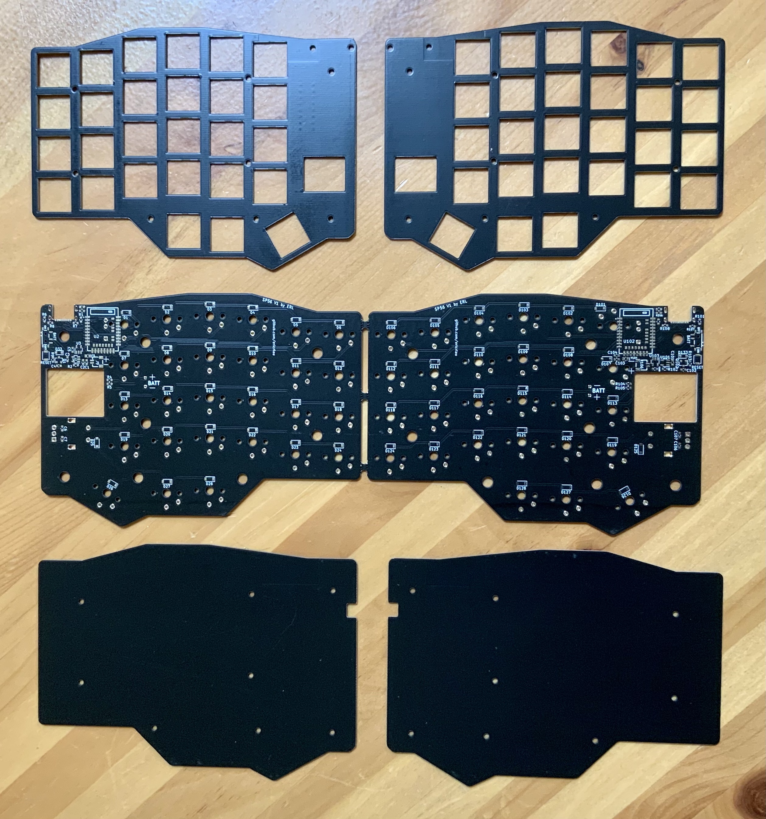
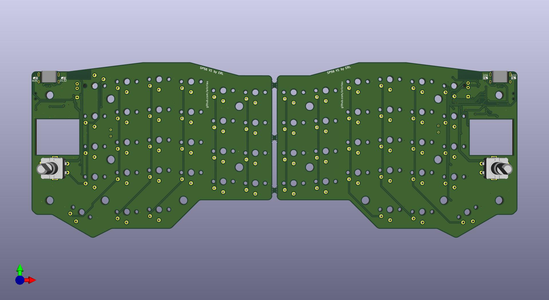
SP56 Bottom is an open-source printed circuit board by ericrlau, from the ericrlau/SP56 repository on GitHub, published under the CC-BY-SA-4.0 licence. It is a 2-layer board of 134.8 × 98 mm with 8 parts on 8 nets.
It belongs with the keyboards and input boards of this library.
:warning: This is a partially tested project. Do not use to create your own copy unless you are willing to debug the hardware and/or firmware.
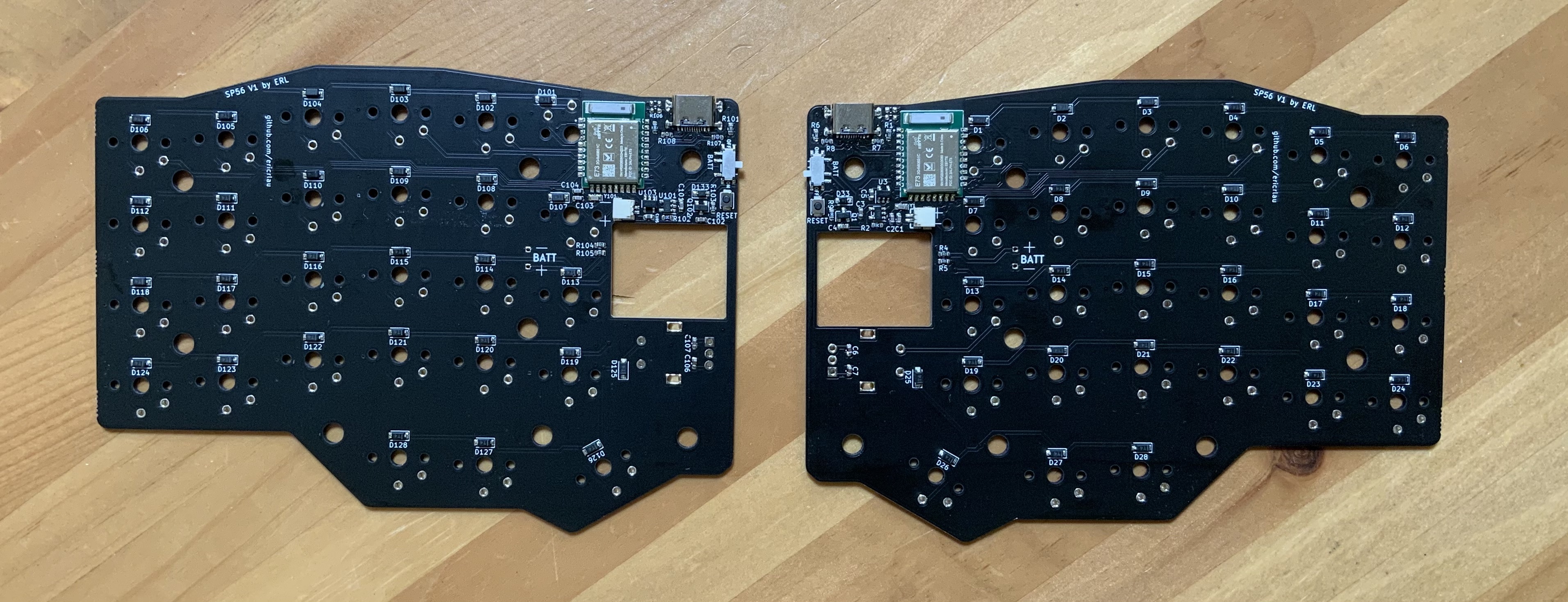
Bootloader is pre-loaded on assembled pcbs. If you source your own BLE module you will need to unlock the module and flash the bootloader using the Nordic nrf command line tool.
$ nrfjprog --recover --log $ nrfjprog -f nrf52 --program firmware/bootloader/COBO_nrf52840_bootloader-0.3.2-184-g64ea299_s140_6.1.1.hex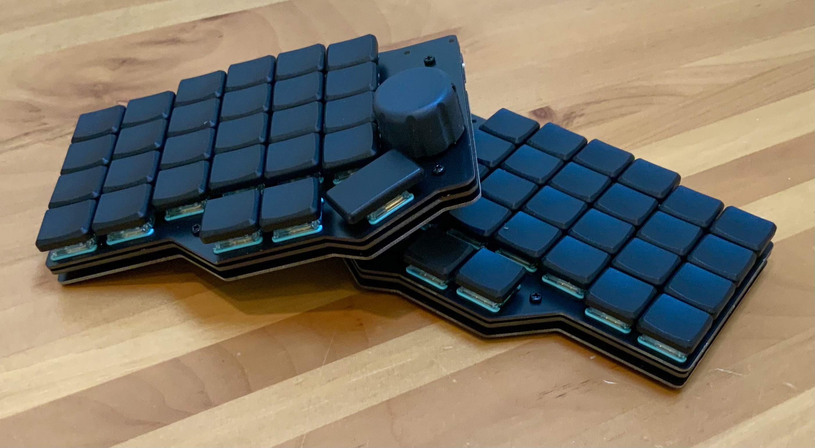
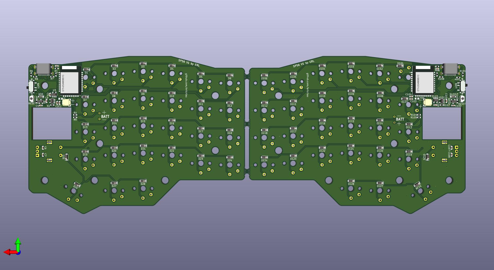
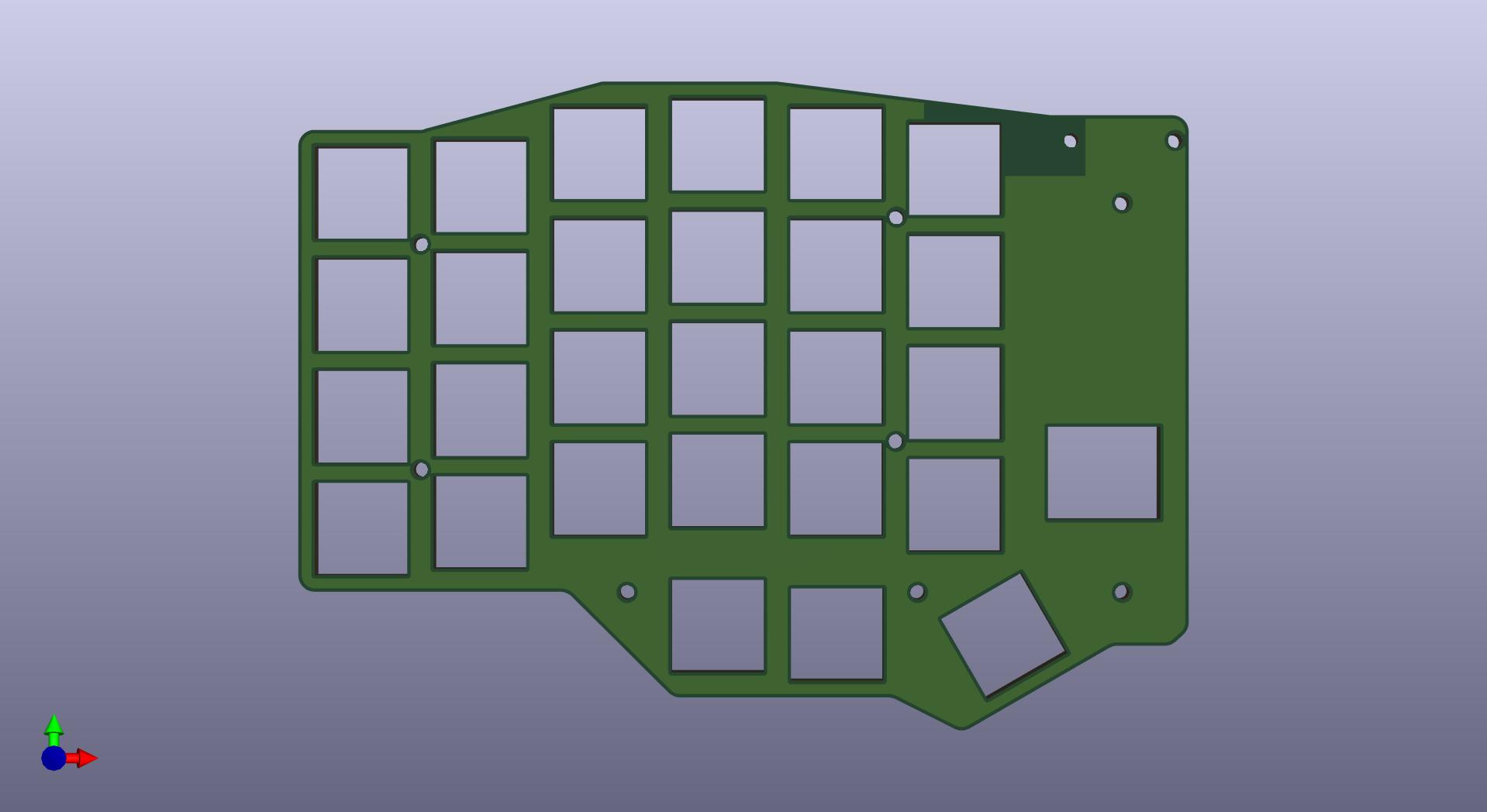
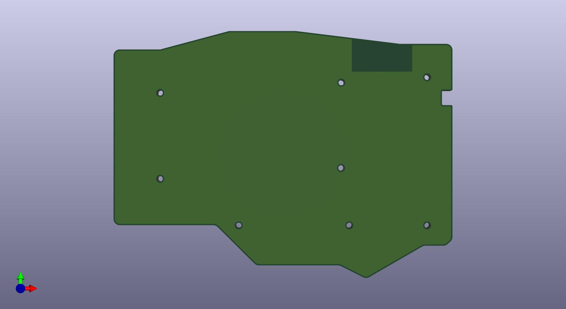
| Qty | Value | Footprint | References |
|---|---|---|---|
| 8 | MountingHole_Pad | MountingHole:MountingHole_2.2mm_M2_DIN965 | H1, H2, H3, H4, H5, H6, H7, H8 |
ericrlau/SP56
Bluetooth low engery keyboard. Layout based on Sofle keyboard with some modifications. NRF52840 powered. Designed around Kaihl Choc switches and spacing.

ericrlau/SP56
Bluetooth low engery keyboard. Layout based on Sofle keyboard with some modifications. NRF52840 powered. Designed around Kaihl Choc switches and spacing.

ericrlau/SP56
Bluetooth low engery keyboard. Layout based on Sofle keyboard with some modifications. NRF52840 powered. Designed around Kaihl Choc switches and spacing.


joeycastillo/Sensor-Watch
A board replacement for the classic Casio F-91W wristwatch

rusefi/rusefi
rusefi - GPL internal combustion engine control unit

hoglet67/RGBtoHDMI
Bare-metal Raspberry Pi project that provides pixel-perfect sampling of Retro Computer RGB/YUV video and conversion to HDMI

shanteacontrols/OpenDeck
A platform for building interactive control and sensing devices using MIDI and OSC built with Zephyr RTOS.

hackclub/OnBoard
💡 Join 1,000 teenagers and make your first PCB with a $100 grant!

dangiu/PicoMemcard
Emulating PSX Memory Card (or controller) using a Raspberry Pi Pico

OLIMEX/DIY-LAPTOP
Do It Yourself Open Source Hardware and Software Modular Hacker's Friendly Laptop
It measures 134.8 × 98 mm and has 2 copper layers, 1.6 mm thick.
8 parts. The full list of its parts is on this page, with links to each part's symbol and footprint where PCBKit's library has them.
From the ericrlau/SP56 repository on GitHub, at the commit this page was made from: the board is PCB/SP56_Bottom/SP56_Bottom.kicad_pcb and its schematic PCB/REF_Panel/REF_Panel.kicad_sch. PCBKit opens the board in the browser, with nothing to install.
Its repository publishes it under the CC-BY-SA-4.0 licence: you may reuse it on that licence's terms (keep the author's notice, and for a copyleft licence share your changes alike).