6 layers290.7 × 322 mm
Board routed golden
epatel/discrete6502
A MOS 6502 CPU rebuilt from 4,051 discrete transistors on a 291x322mm six-layer board that reproduces the original die layout
5,425 parts14

 epatel/discrete650214
A MOS 6502 CPU rebuilt from 4,051 discrete transistors on a 291x322mm six-layer board that reproduces the original die layout
Board presignal is an open-source printed circuit board by epatel, from the epatel/discrete6502 repository on GitHub. It is a 6-layer board of 290.7 × 322 mm with 5,425 parts on 2,624 nets, routed with 7,252 tracks and 3,852 vias.
It is built around the AB4, BSS138K and 1N4148WS, with the AB1, AB10 and AB14 among its other parts. Its parts include 4,051 transistors, 1,110 resistors, 156 capacitors, 67 diodes and 1 IC. It belongs with the retro computing and games boards and the RP2040 and RP2350 boards of this library.



A complete, verified design for a MOS 6502 CPU built from 4,051 discrete surface-mount transistors (3,996 logic + 55 LED drivers), laid out as a 291 × 322 mm six-layer PCB that visually reproduces the original 6502 die — every FET sits at its transistor's die-true position, 55 LEDs blink the register bits in place, and a ring of die-scaled bond pads around the edge takes crocodile clips.
The design is finished and every check passes, but no board has been built yet — nothing here has been proven in copper, only in simulation and geometry. See Status for what that means.
→ Illustrated project introduction — start here if you want the story rather than the build.
Inspired by the MOnSter 6502 (concept only — independently designed and simplified). Logic ground truth is the visual6502 reverse-engineered netlist, captured from photographs of a real decapped 6502.
| Front (the die) | Back (passives + Pico site) |
|---|---|
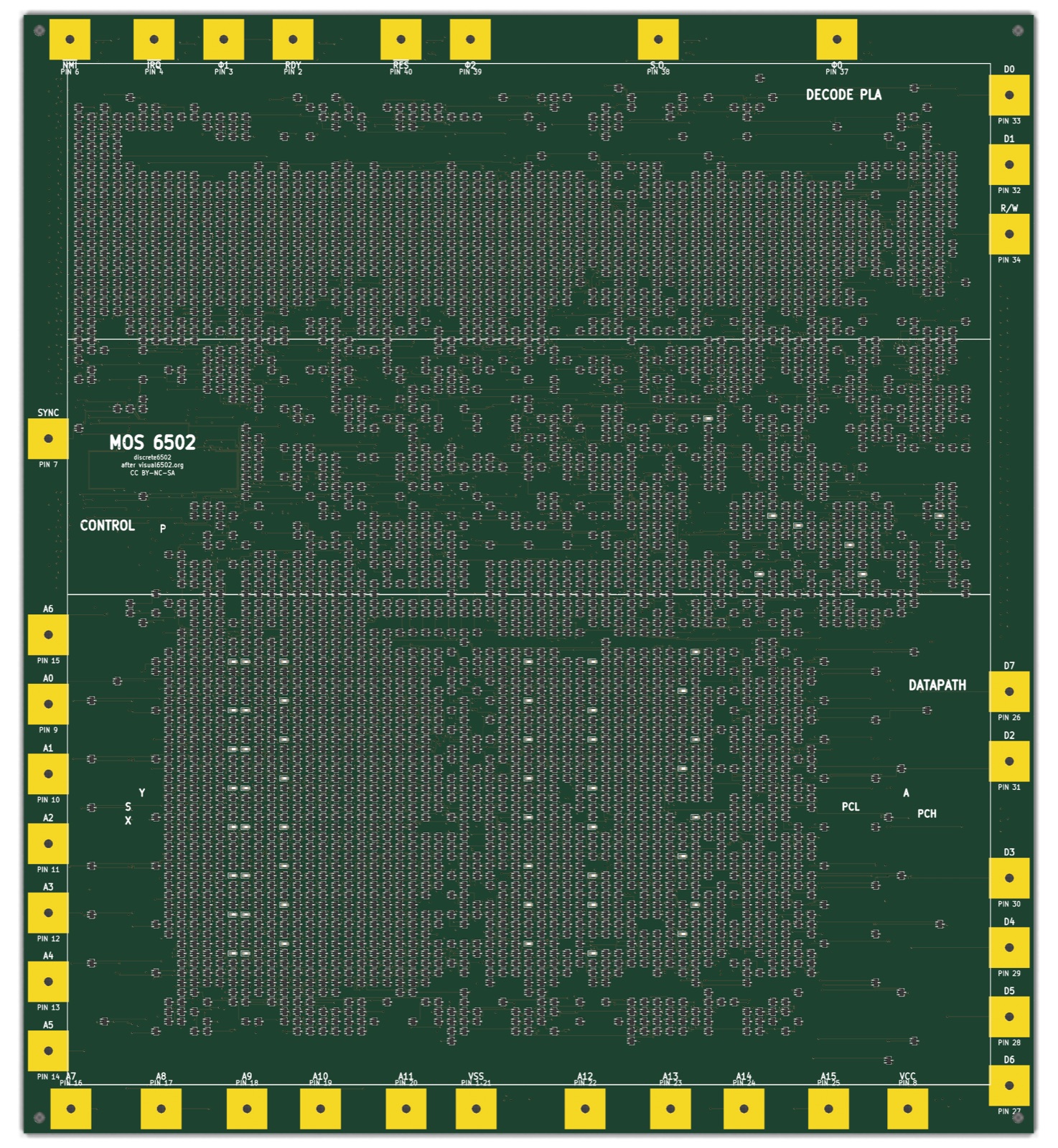 | 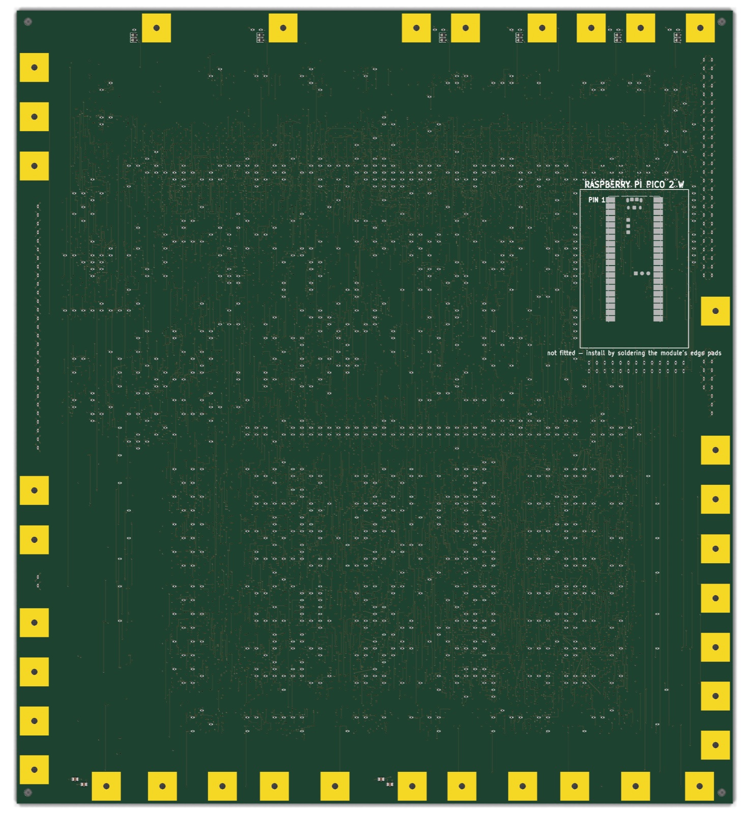 |
Rev A ordered 2026-07-28 and in production — 5 boards, 4 of them assembled.
Both manufacturer confirmation gates passed (PCB stackup verified by measurement,
SMT placement verified on the DFM image).
Release record with file fingerprints and full verification results:
gen/fab/RELEASE.md; step-by-step ordering checklist:
gen/fab/ordering.html. Bring-up (M6) starts when boards arrive.
Verified against the exact board in that package: switch-level equivalence PASS, board-vs-netlist parity 0 errors, independent copper connectivity 0 broken, DRC 0 electrical violations (2 benign items inside the Pico library footprint) and 0 unconnected.
| Milestone | State |
|---|---|
| M1 Research (visual6502 data, MOnSter lessons) | ✅ |
| M2 Feasibility (dynamic NMOS, pass-FET pairs, SPICE) | ✅ |
| M3 Toolchain (KiCad, scripted netlist pipeline) | ✅ |
| M4 Verification (switch-level equivalence, vendor-model SPICE) | ✅ |
| M5 Layout (placement, routing, DRC-clean, fab outputs) | ✅ |
| M6 Fab & bring-up | ⏳ |
Rev A is what is being built. After the order was placed, a defect was found that the
verification chain was structurally unable to see: the transform preserved the netlist's
topology but not its device ratios. Ratioed NMOS needs a weak load against a strong
pull-down; the 1,018 depletion loads correctly became 10 kΩ resistors, but the enhancement-mode
VCC-side FETs kept the same BSS138W as their pull-down — a 1:1 ratio. On the eight data-bus
output drivers that costs 262 mA and 0.90 W per FET (against 220 mA and ~0.3 W ratings) and
leaves the logic low at 1.0–1.9 V against a 1.1–1.5 V threshold, so the stage can read high
when it should read low. Measured in sim/driver_contention.sp;
the corroboration is that it puts the board at ~2 A / ~10 W, which is exactly where the MOnSter
6502 has always been published.
Rev A boards are fixable by hand: 10 kΩ in series with eight FETs, all on the front face in
one column. → Illustrated rework instructions
— true-scale renders of all eight sites generated from the board file, the exact coordinates, the
procedure and its verification steps. (Source: docs/rework-dor-series-r.html.)
Rev B fixes it in the generator. DISCRETE6502_REV_B=1 python3 tools/gen_netlist.py emits a
series resistor for each VCC-side FET that has a pull-down to fight — 142 of the 164, the other
22 being unable to contend at all — sized per net from its gate load (10k where the net drives one
gate, down to 100R on the 13 nF clock nets, all values already in the BOM). None of the 164 turned
out to be a deliberate push-pull driver, so the 1:1 ratio error really is that uniform. The equivalence gate is green on rev B. No rev B board has been made — it needs the
full pipeline re-run from placement onward, so it is a respin rather than a patch. Rev A output
is byte-identical with the flag off, so the fabricated design cannot drift.
sim/fanout_speed.sp).tools/extract_netlist.py): the netlist is also read back out of
the copper — every net label discarded, conductors recovered geometrically from pads,
tracks, vias and zone fills — giving 0 opens and 0 shorts against the intended netlist, and
a netlist that runs the 6502 test program correctly. The copper, read as copper, executes
instructions. Verified to be able to fail: cutting one track reports exactly one open.tools/route_nc.c/.py): a PathFinder-style negotiated-congestion router
— nets route through conflicts, shared cells get iteratively penalized, conflicted nets
rip-up and retry — on a 0.13 mm grid over 4 routing layers, with warm-start checkpoints.
8,421 signal connections routed; the C core does a full negotiation iteration in seconds.pico-controller/ is written and builds, but is untested against hardware
that does not exist yet.Dominated by the NMOS pull-up current, not switching. Component counts are from
gen/netlist.json; the LED figure is simulated (sim/led_tap.sp).
| Contribution | Basis | Typical | Worst case |
|---|---|---|---|
| Pull-up static current | 1,023 × 10 kΩ, 0.50 mA per node held low; ~half low at any moment (worst case: all) | 0.26 A / 1.28 W | 0.51 A / 2.56 W |
| Register LEDs | 55 taps × 1.42 mA; ~half the monitored bits set (worst case: all lit) | 0.04 A / 0.20 W | 0.08 A / 0.39 W |
| Dynamic switching | 109 nF total gate capacitance; 21 nF of it on clock-rate nets, rest at ~15% activity, at 10 kHz | ~9 mW | ~45 mW at 50 kHz |
| Pico 2 W, if VSYS is soldered | ~30 mA at 3.3 V through its buck | 0.02 A / 0.12 W | 0.03 A / 0.15 W |
| Total @ 5 V — ⚠️ incomplete, see below | ≈ 0.32 A / 1.6 W | ≈ 0.63 A / 3.2 W | |
| Total @ 5 V, as actually built | driver contention added | ≈ 2.1 A / ≈ 10.4 W |
SUPERSEDED 2026-08-01 — this table is wrong by about 6x. It counts pull-up resistors, LEDs and switching only. It does not count driver contention: the eight data-bus output drivers hold a VCC-side FET and a pull-down FET on together for 47–93% of the time, drawing 262 mA each at 5 V. Measured in
sim/driver_contention.sp, that adds +1.76 A and +8.8 W, taking the board to ≈2.1 A / ≈10.4 W — which is where the MOnSter 6502's published 2 A / 10 W was all along. A 1 A supply is not enough; use 3 A. Full analysis and the rework that fixes it: "Driver contention" inproject-plan.md.
A 5 V / 1 A bench supply covers even the worst case. Use 3 A — see the
correction above. The old comparison line read "compare the original MOnSter 6502
at ~10 W", which in hindsight was the clue: same logic, same style, and it should
never have been six times cheaper. With contention counted, this board lands in
the same place. The 8.8 W of contention is not spread over the 900 cm² board
either — it is concentrated in eight SOT-323s in one column, which is the whole
problem.
At 3.3 V (the diagnostic fallback rail — bring-up starts at 5 V, see
pico-controller/README.md):
≈ 0.19 A / 0.64 W typical, 0.38 A / 1.3 W worst case. The LEDs there draw
0.67 mA each instead of 1.42 mA, because the 2.2 kΩ ballast has 1.4 V less
headroom above the LED's ~1.85 V forward drop — 47% of the current, but only
about 20% less perceived brightness (perception goes roughly as the cube root
of luminous output): dimmer, still perfectly readable.
Transient behaviour is more interesting than the average: the cclk net alone
carries 13 nF of gate load (482 gates), so clock edges pull ~50–100 mA for a
microsecond or two. That is what the 96 distributed 100 nF decouplers and 4 ×
10 µF bulk caps are for — they hold the rail to ~10 mV of droop across an edge.
project-plan.md — goals, milestones, decision log, current handoff (start here)cards/ — deep-dive notes per topic (architecture, layout, verification, …)data/visual6502/ — the reverse-engineered netlist source datatools/ — the entire generation pipeline: netlist transform, die placement, power routing,
the negotiated-congestion signal router, finishing passes, silkscreen, verificationsim/ — ngspice testbenches: pass-pair latch, 3.3 V validation, LED brightness, fanout speedgen/ — generated artifacts: netlist, boards (board_routed_golden.kicad_pcb), renders,
and the JLCPCB fabrication package (gen/fab/)The full pipeline, in order (KiCad 10's bundled python for board steps):
python3 tools/gen_netlist.py         # visual6502 data -> netlist (+ invariant checks)
python3 tools/switchsim.py           # equivalence gate: must stay green
<kicad-python> tools/gen_pcb.py      # die-true placement, board setup
<kicad-python> tools/route_power.py  # planes + ~3,700 stitch vias
<kicad-python> tools/route_power_finish.py   # (on the presignal snapshot)
<kicad-python> tools/route_nc.py     # signal routing (hours; checkpointed)
<kicad-python> tools/fix_same_net_vias.py
<kicad-python> tools/fix_via_pairs.py
<kicad-python> tools/enlarge_vias.py  # 0.30mm drills for JLC's free class
<kicad-python> tools/add_silk.py
<kicad-python> tools/check_parity.py && tools/check_gaps.py + kicad-cli drc
<kicad-python> tools/extract_netlist.py   # rebuild the netlist from copper (LVS)
python3 tools/switchsim.py           # now also simulates the extracted netlist
See cards/layout.md for the rules and hard-won caveats behind each step.
Copyright © 2026 Edward Patel.
This project is licensed CC BY-NC-SA 4.0 (Creative Commons
Attribution-NonCommercial-ShareAlike 4.0 International) — the full legal code is in
LICENSE. It covers everything in the repository: the board design and
generated artifacts in gen/, the generation and verification tools in tools/, the SPICE
testbenches in sim/, the Pico firmware in pico-controller/, and the documentation.
In short: use it, modify it and share it, with attribution, for non-commercial purposes, and share derivatives under the same terms.
The licence is inherited rather than chosen. The design's ground truth is the visual6502
project's netlist data, whose segdefs.js is itself CC BY-NC-SA, so this work carries the
same terms forward. Attribution is owed to visual6502.org, which
traced a real 6502 die photograph by photograph and made the result public.
The MOnSter 6502 by Eric Schlaepfer and Evil Mad Scientist Laboratories proved a discrete 6502 is possible and is gratefully acknowledged as inspiration. This is an independent design and is not affiliated with that project.
| Qty | Value | Footprint | References |
|---|---|---|---|
| 4051 | BSS138K | SOT-323_SC-70 | Q1, Q10, Q100, Q101, Q1000, Q1001, Q1002, Q1003, Q1004, Q1005, Q1006, Q1007, Q1008, Q1009, Q1010, Q1011 +4035 |
| 1023 | 10k | R_0402_1005Metric | R1, R10, R100, R101, R1000, R1001, R1002, R1003, R1004, R1005, R1006, R1007, R1008, R1009, R1010, R1011 +1007 |
| 96 | 100nF | C_0402_1005Metric | C1, C2, C10, C11, C12, C13, C14, C15, C16, C17, C18, C19, C20, C21, C22, C23 +80 |
| 56 | 100pF-DNP | C_0402_1005Metric | C101, C102, C103, C104, C105, C106, C107, C108, C109, C110, C111, C112, C113, C114, C115, C116 +40 |
| 55 | 2.2k | R_0402_1005Metric | R1019, R1020, R1021, R1022, R1023, R1024, R1025, R1026, R1027, R1028, R1029, R1030, R1031, R1032, R1033, R1034 +39 |
| 55 | LED_RED | LED_0603_1608Metric | D1, D2, D10, D11, D12, D13, D14, D15, D16, D17, D18, D19, D20, D21, D22, D23 +39 |
| 26 | 1k | R_0402_1005Metric | R1085, R1086, R1087, R1088, R1089, R1090, R1091, R1092, R1093, R1094, R1095, R1096, R1097, R1098, R1099, R1100 +10 |
| 12 | 1N4148WS | D_SOD-323 | D56, D57, D58, D59, D60, D61, D62, D63, D64, D65, D66, D67 |
| 6 | 100R | R_0402_1005Metric | R1074, R1075, R1076, R1077, R1078, R1079 |
| 4 | 10uF | C_0805_2012Metric | C97, C98, C99, C100 |
| 4 | MountingHole_3.2mm_M3 | MountingHole_3.2mm_M3 | H1, H2, H3, H4 |
| 1 | AB0 | TestPoint_THTPad_4.0x4.0mm_Drill2.0mm | TP1 |
| 1 | AB1 | TestPoint_THTPad_4.0x4.0mm_Drill2.0mm | TP2 |
| 1 | AB10 | TestPoint_THTPad_4.0x4.0mm_Drill2.0mm | TP11 |
| 1 | AB11 | TestPoint_THTPad_4.0x4.0mm_Drill2.0mm | TP12 |
| 1 | AB12 | TestPoint_THTPad_4.0x4.0mm_Drill2.0mm | TP13 |
| 1 | AB13 | TestPoint_THTPad_4.0x4.0mm_Drill2.0mm | TP14 |
| 1 | AB14 | TestPoint_THTPad_4.0x4.0mm_Drill2.0mm | TP15 |
| 1 | AB15 | TestPoint_THTPad_4.0x4.0mm_Drill2.0mm | TP16 |
| 1 | AB2 | TestPoint_THTPad_4.0x4.0mm_Drill2.0mm | TP3 |
| 1 | AB3 | TestPoint_THTPad_4.0x4.0mm_Drill2.0mm | TP4 |
| 1 | AB4 | TestPoint_THTPad_4.0x4.0mm_Drill2.0mm | TP5 |
| 1 | AB5 | TestPoint_THTPad_4.0x4.0mm_Drill2.0mm | TP6 |
| 1 | AB6 | TestPoint_THTPad_4.0x4.0mm_Drill2.0mm | TP7 |
| 1 | AB7 | TestPoint_THTPad_4.0x4.0mm_Drill2.0mm | TP8 |
| 1 | AB8 | TestPoint_THTPad_4.0x4.0mm_Drill2.0mm | TP9 |
| 1 | AB9 | TestPoint_THTPad_4.0x4.0mm_Drill2.0mm | TP10 |
| 1 | CLK0 | TestPoint_THTPad_4.0x4.0mm_Drill2.0mm | TP25 |
| 1 | CLK1OUT | TestPoint_THTPad_4.0x4.0mm_Drill2.0mm | TP26 |
| 1 | CLK2OUT | TestPoint_THTPad_4.0x4.0mm_Drill2.0mm | TP27 |
| 1 | DB0 | TestPoint_THTPad_4.0x4.0mm_Drill2.0mm | TP17 |
| 1 | DB1 | TestPoint_THTPad_4.0x4.0mm_Drill2.0mm | TP18 |
| 1 | DB2 | TestPoint_THTPad_4.0x4.0mm_Drill2.0mm | TP19 |
| 1 | DB3 | TestPoint_THTPad_4.0x4.0mm_Drill2.0mm | TP20 |
| 1 | DB4 | TestPoint_THTPad_4.0x4.0mm_Drill2.0mm | TP21 |
| 1 | DB5 | TestPoint_THTPad_4.0x4.0mm_Drill2.0mm | TP22 |
| 1 | DB6 | TestPoint_THTPad_4.0x4.0mm_Drill2.0mm | TP23 |
| 1 | DB7 | TestPoint_THTPad_4.0x4.0mm_Drill2.0mm | TP24 |
| 1 | IRQ | TestPoint_THTPad_4.0x4.0mm_Drill2.0mm | TP30 |
| 1 | NMI | TestPoint_THTPad_4.0x4.0mm_Drill2.0mm | TP31 |
| 1 | Pico2_W_site | RaspberryPi_Pico_W_SMD | U1 |
| 1 | RDY | TestPoint_THTPad_4.0x4.0mm_Drill2.0mm | TP29 |
| 1 | RES | TestPoint_THTPad_4.0x4.0mm_Drill2.0mm | TP28 |
| 1 | RW | TestPoint_THTPad_4.0x4.0mm_Drill2.0mm | TP32 |
| 1 | SO | TestPoint_THTPad_4.0x4.0mm_Drill2.0mm | TP34 |
| 1 | SYNC | TestPoint_THTPad_4.0x4.0mm_Drill2.0mm | TP33 |
| 1 | VCC | TestPoint_THTPad_4.0x4.0mm_Drill2.0mm | TP36 |
| 1 | VSS | TestPoint_THTPad_4.0x4.0mm_Drill2.0mm | TP35 |
epatel/discrete6502
A MOS 6502 CPU rebuilt from 4,051 discrete transistors on a 291x322mm six-layer board that reproduces the original die layout

embeddedos-org/eCAD-Hardware-Products
Hardware designs + EE docs + Board datasheets of Multiple products


sastles-com/isolation-sphere-solo-xiao
球体 LED ディスプレイのファームウェア。server なし (solo) と server あり (配信) の両方を 1 つの バイナリで動かす。


Chethien1912/Shrimp-Feed-Grinder-Motor-Driver-PCB
Board điều khiển động cơ máy xay thức ăn cho tôm

GauravSh7/tracewise-pcb-validator
AI-assisted PCB design validation platform for early-stage KiCad board review.

MateoCignetti/ProyectoFinal
Esta obra está bajo una [Licencia Creative Commons Atribución-NoComercial-CompartirIgual 4.0 Internacional][cc-by-nc-sa].

AssaadMH/mcu-sensor-firmware-studies
A set of small but complete embedded programs — PIC instrumentation with LCD readout, and an NFC tag reader.
It measures 290.7 × 322 mm and has 6 copper layers, 1.6 mm thick.
5,425 parts, built around the AB4, BSS138K, 1N4148WS and AB1. The full list of its parts is on this page, with links to each part's symbol and footprint where PCBKit's library has them.
From the epatel/discrete6502 repository on GitHub, at the commit this page was made from: the board is gen/board_presignal.kicad_pcb. PCBKit opens the board in the browser, with nothing to install.
Its repository states no licence, so its author keeps all rights: ask epatel before reusing the design.