2 layers65 × 30 mm
Max3421e rpi uhat
StarGate01/max3421e-rpi-uhat
A uHAT for the Rapberry Pi (Zero), which adds a second USB 2.0 controller over SPI, using the MAX3421E chip.
23 parts1MPL-2.0

 emwjacobson/USB_Wifi_Switch
This project aims to create a wifi-enabled module containing 2 individually switchable USB ports.
USB Switch is an open-source printed circuit board by emwjacobson, from the emwjacobson/USB_Wifi_Switch repository on GitHub. It is a 2-layer board of 38.1 × 63.5 mm with 31 parts on 43 nets, routed with 175 tracks and 35 vias.
It is built around the ESP-12F(ESP8266MOD), AMS1117-3.3 and RC0603JR-0710KL, with the 201007F100LT4E, RC0603FR-07330RL and 19-217/GHC-YR1S2/3T among its other parts. Its parts include 11 resistors, 6 capacitors, 5 connectors, 4 ICs and 2 diodes. It belongs with the ESP8266 boards of this library.


This project aims to create a wifi-enabled module containing 2 individually switchable USB ports.
There are software-programmable LEDs that can be used to show the current status of each port.
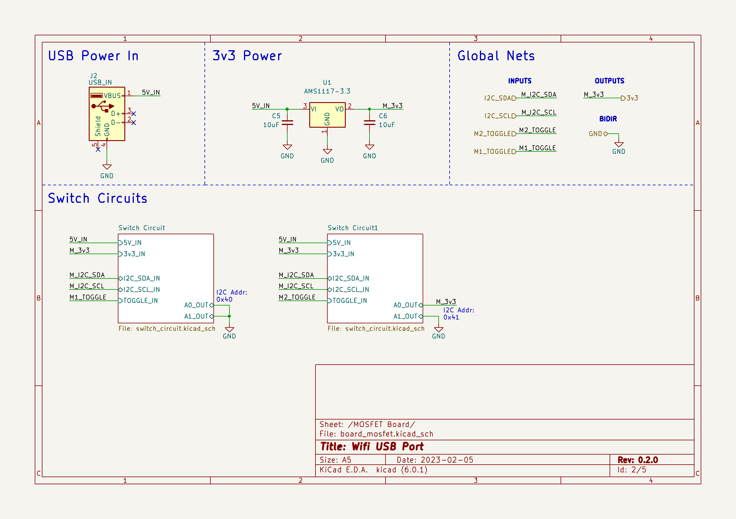
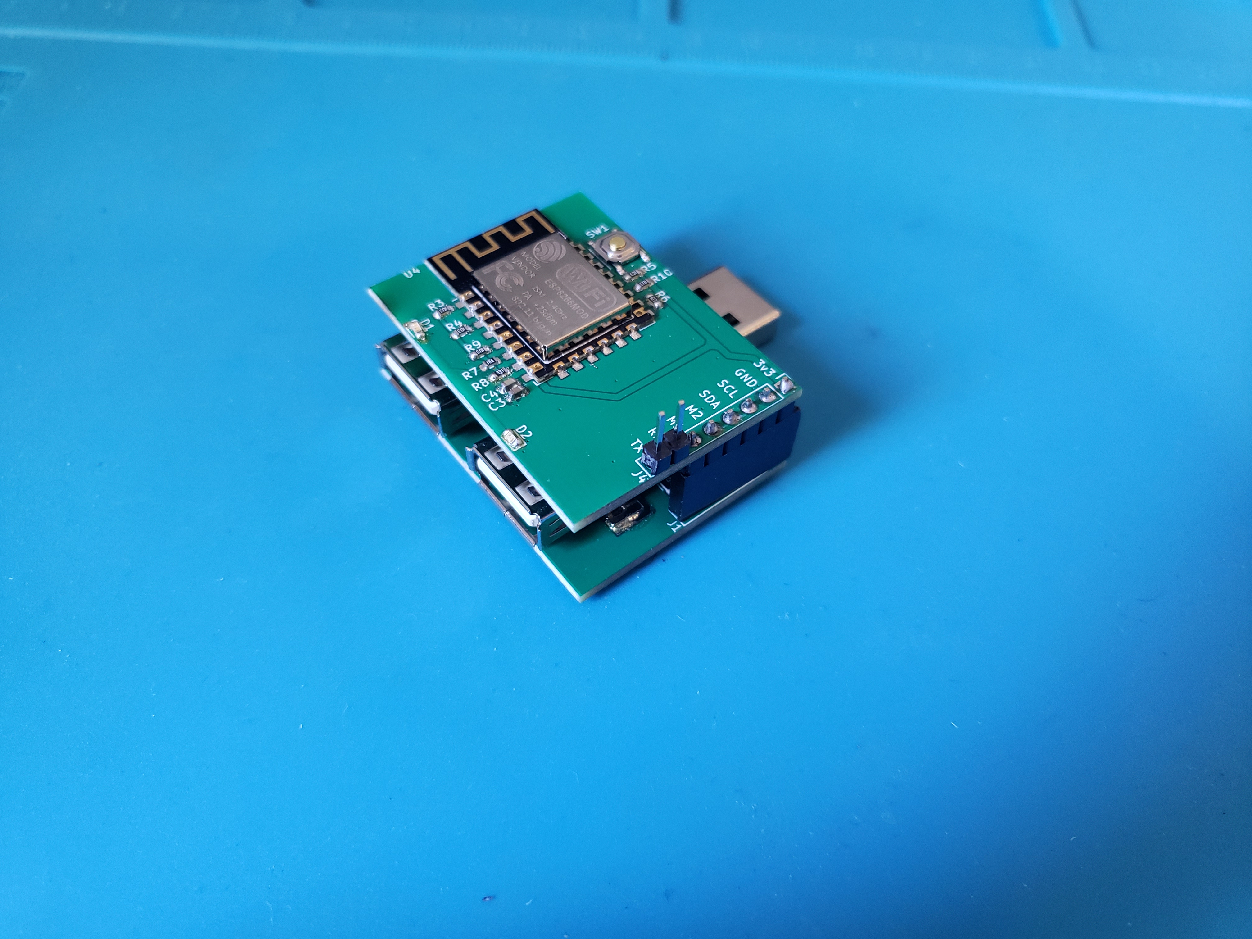
The design is broken up into 2 parts, the MOSFET board and the Control board. In the assembled product, these are connected using headers to create a 2-layered design.
The control board consists of the ESP8266 module that controls the LEDs as well as the 2 MOSFETs on the MOSFET board.
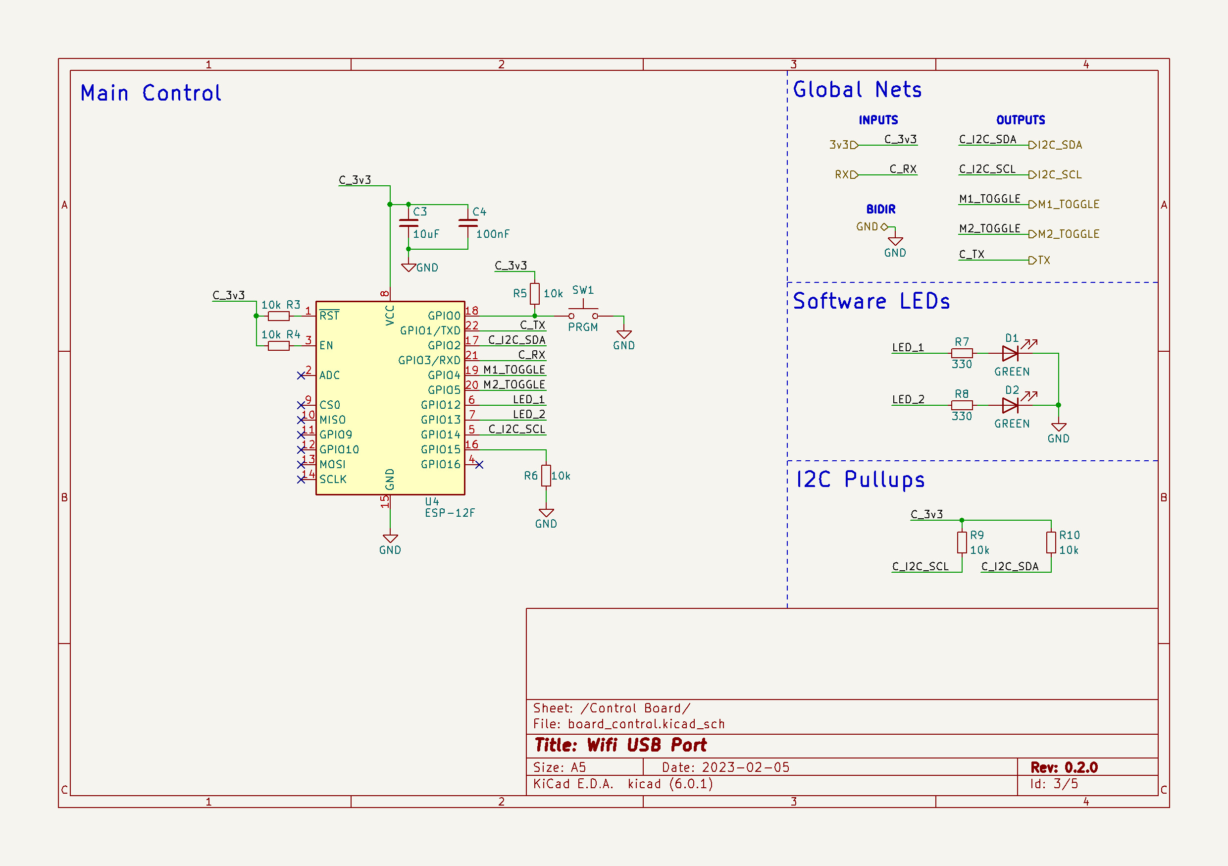
As the name implies, this is the board that holds 2 copies of the power switching circuit as well as a 3.3v regular for the Control board.
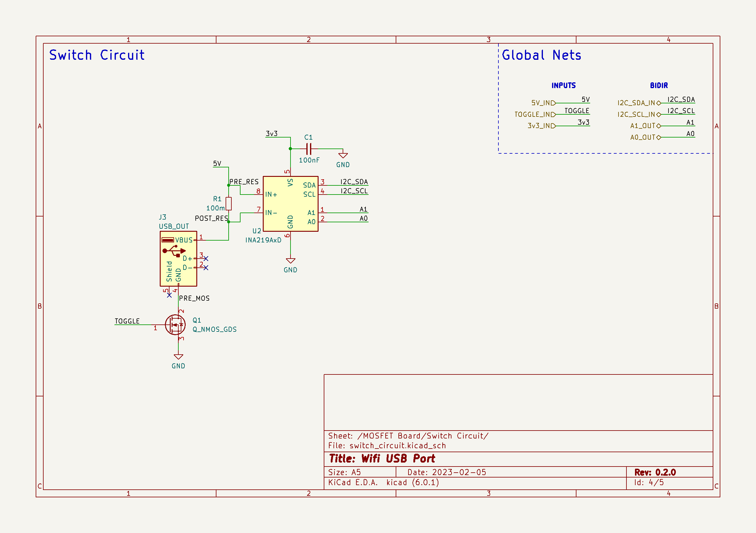
There are 2 copies of this circuit, as shown in the MOSFET Board schematic. The switch circuit contains
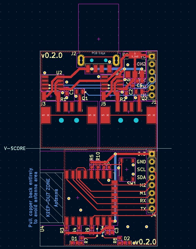
The PCB design was made as a single-sided component design, as it's easy enough for me to hand-assemble with a hot-air reflow station.
There is a v-score that is intended to be used to split the board into it's two halves and stacked with headers.
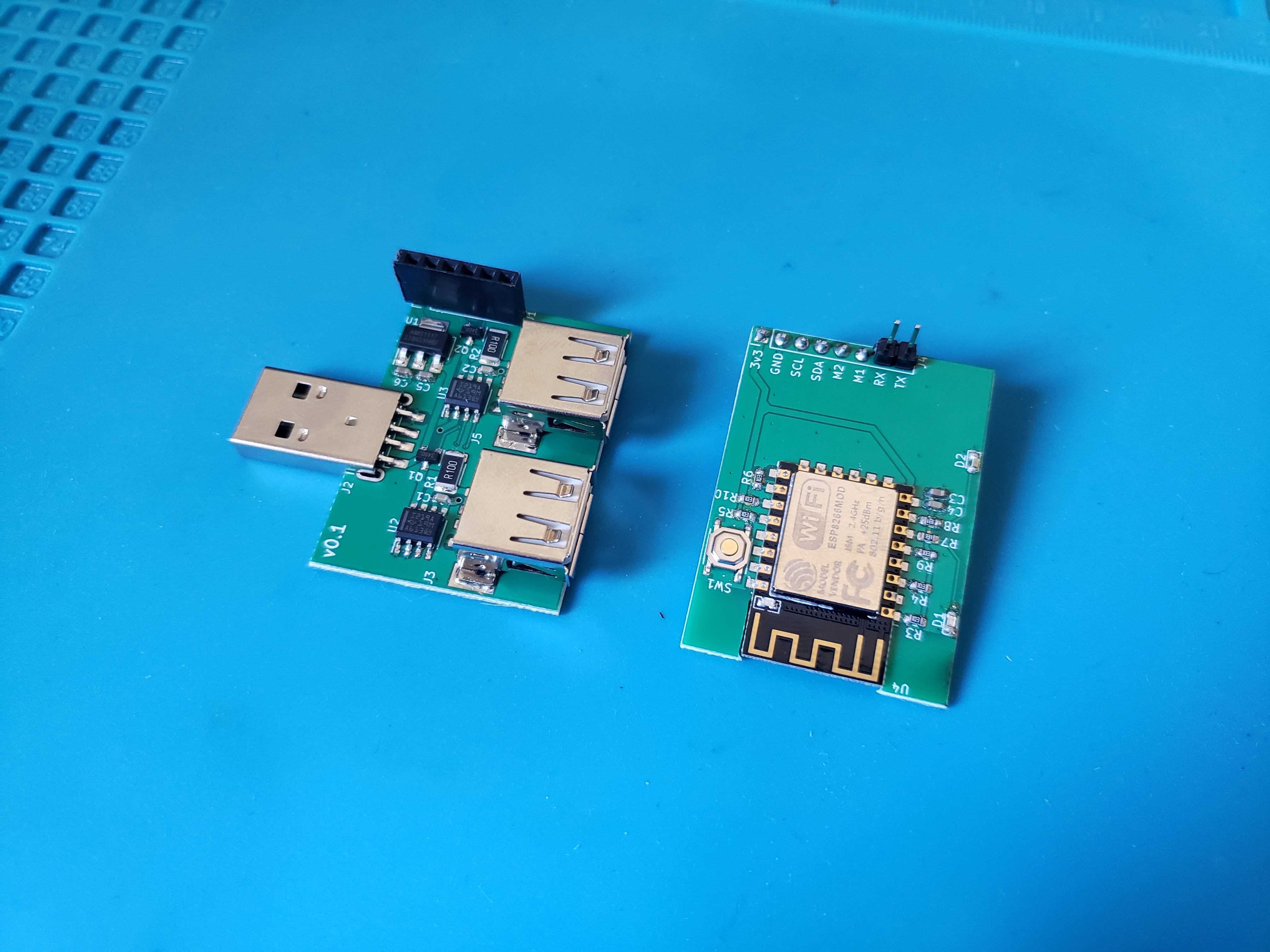
Currently I have an older version assembled and working on auto-charging a tablet I use as a Home Assistant dashboard. That board is v0.1.2, and does not have correct voltage reading. When I ver v0.2.0 ordered and assembled, I hope to post a photo of it.
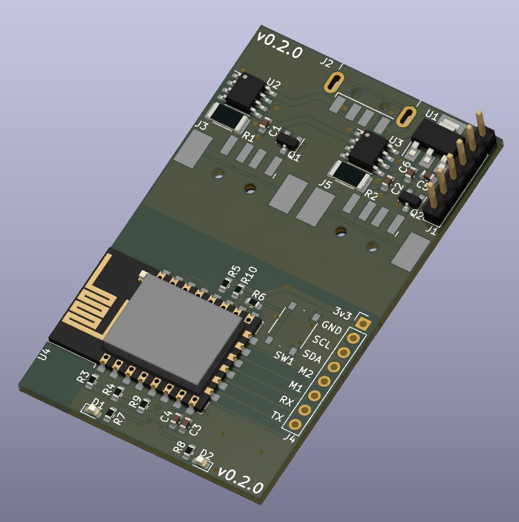
I do have images of an even older version, v0.1, that I have since disassembled and reworked to be the v0.1.2 board that I currently use.
| Qty | Value | Footprint | References |
|---|---|---|---|
| 6 | 10k | Resistor_SMD:R_0603_1608Metric | R3, R4, R5, R6, R9, R10 |
| 3 | 100nF | Capacitor_SMD:C_0603_1608Metric | C1, C2, C4 |
| 3 | 10uF | Capacitor_SMD:C_0603_1608Metric | C3, C5, C6 |
| 2 | 100m | Resistor_SMD:R_2010_5025Metric | R1, R2 |
| 2 | 330 | Resistor_SMD:R_0603_1608Metric | R7, R8 |
| 2 | GREEN | LED_SMD:LED_0603_1608Metric | D1, D2 |
| 2 | INA219AxD | Package_SO:SOIC-8_3.9x4.9mm_P1.27mm | U2, U3 |
| 2 | Q_NMOS_GDS | Library:YJL3400A | Q1, Q2 |
| 2 | USB_OUT | Library:904-131A2032S10100 | J3, J5 |
| 1 | 100 | Resistor_SMD:R_0603_1608Metric | R11 |
| 1 | AMS1117-3.3 | Package_TO_SOT_SMD:SOT-223-3_TabPin2 | U1 |
| 1 | Conn_01x06 | Connector_PinHeader_2.54mm:PinHeader_1x06_P2.54mm_Vertical | J1 |
| 1 | Conn_01x08 | Connector_PinHeader_2.54mm:PinHeader_1x08_P2.54mm_Vertical | J4 |
| 1 | ESP-12F | RF_Module:ESP-12E | U4 |
| 1 | PRGM | Library:TS-1187A-B-A-B | SW1 |
| 1 | USB_IN | Library:U217-041N-4BV81 | J2 |
StarGate01/max3421e-rpi-uhat
A uHAT for the Rapberry Pi (Zero), which adds a second USB 2.0 controller over SPI, using the MAX3421E chip.

gslee-dev/portpulse
USB replug test dongle with KiCad hardware, CH552 firmware, and native C host


elagil/net-bmp
An Ethernet-connected SWD/JTAG debug adapter (blackmagic probe)
It measures 38.1 × 63.5 mm and has 2 copper layers, 1.6 mm thick.
31 parts, built around the ESP-12F(ESP8266MOD), AMS1117-3.3, RC0603JR-0710KL and 201007F100LT4E. The full list of its parts is on this page, with links to each part's symbol and footprint where PCBKit's library has them.
From the emwjacobson/USB_Wifi_Switch repository on GitHub, at the commit this page was made from: the board is USB_Switch.kicad_pcb and its schematic USB_Switch.kicad_sch. PCBKit opens the board in the browser, with nothing to install.
Its repository states no licence, so its author keeps all rights: ask emwjacobson before reusing the design.