4 layers120 × 75 mm
Portapack h1
portapack-mayhem/mayhem-firmware
The firmware for the HackRF+PortaPack H1/H2/H4/H4M
111 parts5.5kGPL-3.0

 emtenet/max-v-fuse-map
Altera MAX V Fuse Map (by experiment)
Dev board is an open-source printed circuit board by emtenet, from the emtenet/max-v-fuse-map repository on GitHub, published under the ISC licence. It is a 2-layer board of 96.5 × 96.5 mm with 40 parts on 123 nets, routed with 1,250 tracks and 68 vias.
It is built around the 5M160ZT100C5N, 5M240ZT144C5N and 5M40ZE64C5N. Its parts include 16 connectors, 15 capacitors and 5 ICs. It belongs with the microcontroller boards boards of this library.


This is a puzzle. Can I work out the fuse map of MAX V devices by feeding the Quartus tools and observing the outputs?
My experiments are being run in the following environment.
A mapping to and from fuse numbers, locations & names is encoded in fuse map.
The following mux mappings are encoded:
Some MUX databases have been collected:
database/*.lab-interconnectdatabase/*.iob-interconnectdatabase/*.c4-interconnectdatabase/*.r4-interconnectdatabase/*.ufm-interconnectAll known fuses are also dumped for import into rust tools:
{device, reset}This enables the device wide reset pin that resets all registers in the device
{device, output_enable}This enables the device wide output enable pin to control the output enable for every output pin on the device.
{global(), row, off} and {global(), {column, #}, off}Each of the four global clock networks are driven horizontally (row) and then to each column. Unused clock networks are turned off either at individual columns or for the whole row.
{global(), internal}Each of the global clock networks can be driven from either:
This fuse selects the internal interconnects.
{{global, X, Y}, N, from3, mux#}, {{global, X, Y}, N, from4/6, mux#} and {{global, X, Y}, N, invert}Selects an interconnect into each of the four global networks.
For the 5M240Z, 6 x 3 muxes are repurposed from unused IOC output and enable muxes.
For other densities, 4 x 3 muxes selecting from 10 interconnects are located in the special UFM blocks.
{user_code, bit()}There are 32 bits of user oode numbered LSB (0) to MSB (31).
The user code bits are stored in the POF file inverted,
so a user code bit of 1 is stored as a 0.
{iob(), {interconnect, #}, direct_link}Selects a direct-link from a neighbouring LAB onto an IOB's interconnect.
Only applicable for IOBs on the left and right sides.
Not used at the same time as the interconnect muxes below.
{iob(), {interconnect, #}, from4, mux#}, {iob(), {interconnect, #}, from3, mux#} and {iob(), {interconnect, 8/17}, from4, gclk}Selects a direct-link, C4 or R4 onto an IOB's interconnect.
Not used at the same time as the dedicated direct-link above.
Each interconnect has a two dimentional mux of size 4 x 3 selecting from 12 alternative sources.
As a special case, row interconnects 8 and 17 have an extra fuse expanding the mux to size 5 x 3. The extra 3 alternatives source from the global clock networks.
{ioc(), input_off}The IOC input is turned off when the POF but is 0.
This could also be called output only.
{ioc(), output3, mux#} and {ioc(), output4/6, mux#}The IOC outputs are selected from local interconnects via two dimentional muxes. Side IOCs have one of size 3, and the other of size 6. Top/bottom IOCS have one of size 3, and the other of size 4.
These muxes are one-cold.
For example the fuses
{ioc(), output6, mux2} and {ioc(), output3, mux1}
select local interconnect 7.
For example the fuses
{ioc(), output4, mux3} and {ioc(), output3, mux2}
select local line 9.
{ioc(), fast_out}Selects output value from fast-out link of neighbouring LAB instead of via the output muxes.
{ioc(), output_invert}The IOC output is inverted when the POF but is 0.
{ioc(), enable3, mux#} and {ioc(), enable4/6, mux#}The IOC output enables are selected from local interconnects.
See {ioc(), output#, mux#} for details.
{ioc(), enable_invert}The IOC is an output when the POF but is 0.
{ioc(), bus_hold} and {ioc(), weak_pull_up}Each IOC can have bus-hold or weak pull-up enabled.
The feature is enabled when the POF bit is 0.
Warning: only enable one at a time.
{ioc(), low_current_0} and {ioc(), low_current_1}Drive strength of IOC outputs can be minimum or maximum current.
Default drive strength is maximum current.
A low current strength is enabled with a POF bit of 0.
NOTE: Both fuses are always the same as each other.
{ioc(), fast_slew_rate}Slew Rate of IOC outputs is fast with a POF bit of 0.
{ioc(), input_delay}Input delay on IOC inputs enabled with a POF bit of 0.
{ioc(), open_drain}Open-Drain outputs enabled with a POF bit of 0.
{ioc(), pci_compliance}PCI compliant outputs enabled with a POF bit of 0.
NOTE: Only avaailable in Bank 3 of 5M1270Z and 5M2210Z.
{ioc(), schmitt_trigger}Schmitt Trigger on IOC inputs enabled with a POF bit of 0.
NOTE: Also enabled when in output mode.
{lab(), {interconnect, #}, direct_link}Selects a direct-link from a neighbouring LAB onto a LAB's interconnect.
Not used at the same time as the interconnect muxes below.
{lab(), {interconnect, #}, from4, mux#}, {lab(), {interconnect, #}, from3, mux#} and {lab(), {interconnect, 12/25}, from4, gclk}Selects a direct-link, C4 or R4 onto a LAB's interconnect.
Not used at the same time as the dedicated direct-link above.
Each interconnect has a two dimentional mux of size 4 x 3 selecting from 12 alternative sources.
As a special case, interconnects 12 and 25 have an extra fuse expanding the mux to size 5 x 3. The extra 3 alternatives source from the global clock networks.
{lab(), clk#, global#} and {lab(), clk#, control}Each LAB's clk# can be selected fron the four global signals (0..3) or a control line.
These fuses form a one-shot mux with the active selection with a bit of 0.
{lab(), clk1, control_0_not_1}When the LAB's clk1 line is selected from a control line.
The specific control line selected is:
0 bit selects 0,1 bit selects 1.{lab(), clk2_a_load, control_3_not_2}The LAB's clk2 & a-load lines share a common control source.
When the LAB's clk2 / a-load line is selected from a control line.
The specific control line selected is:
0 bit selects 3,1 bit selects 2.{lab(), clk#, invert}The LAB's clk# line is inverted.
{lab(), ena1, off}This turns off the LAB's ena1 line. LC's are then continuously enabled.
{lab(), ena1, control_3_not_2}This selects the LAB's ena1 line from either:
0 bit selects control line 31 bit selects control line 2{lab(), ena1, invert}This inverts the LAB's ena1 line.
{lab(), ena2, off}This turns off the LAB's ena2 line. LC's are then continuously enabled.
{lab(), ena2_s_load, control_0_not_1}The LAB's ena2 & s-load lines share a common control source.
When the LAB's ena2 / s-load line is selected from a control line.
The specific control line selected is:
0 bit selects 0,1 bit selects 1.{lab(), ena2_s_load, invert}The LAB's ena2 & s-load lines share a common inversion.
The LAB's ena2 / s-load line is inverted.
{lab(), a_clr, global#}Only one of the two a-clr# lines can select from a global line.
This mux is common to those two lines and selected by {lab(), a_clr#, global}.
These fuses form a one-shot mux with the active selection with a bit of 0.
{lab(), a_clr#, off}Turns of the LAB's a-clr# line.
{lab(), a_clr#, global}The LAB's a-clr# line is selected from one of the global lines (also when off).
Alternatively the line is selected from a control line.
{lab(), a_clr#, control_5_not_4}When the LAB's a-clr# line is selected from a control line.
The specific control line selected is:
0 bit selects 5,1 bit selects 4.{lab(), a_clr#, invert}The LAB's a-clr# line is inverted.
{lab(), a_load, control}The LAB's a-load line is selected from one of the control lines.
{lab(), a_load, invert}The LAB's a-load line is inverted.
{lab(), s_clr, control}The LAB's s-clr line is selected from one of the control lines.
{lab(), s_clr, invert}The LAB's s-clr line is inverted.
{lab(), s_clr, control_5_not_4}When the LAB's s-clr line is selected from a control line.
The specific control line selected is:
0 bit selects 5,1 bit selects 4.{lab(), s_load, control}The LAB's s-load line is selected from one of the control lines.
{lab(), s_load, not_always}It has a bit 0 when the s-load is disconnected or connected to a signal.
It has a bit 1 when the s-load line is a constant 1.
{lab(), invert_a}The LAB's invert-a line (addnsub) is enabled.
{lab(), invert_a, control_4_not_3}When the LAB's invert-a line is selected from a control line.
The specific control line selected is:
0 bit selects 3,1 bit selects 4.{lab(), carry_in, invert_a}The LAB's carry-in is selected from:
0 bit selects from the previous LAB`s carry-out signal,1 bit selects from the LAB's invert-a control line.{lc(), clk2}Each LC can select between two LAB wide clocks, clk1 & clk2.
This fuse selects clk2.
{lc(), a_clr1}Each LC can select between two LAB wide a-clrs, a-clr1 & a-clr2.
This fuse selects a-clr1.
It also elects out of the LAB's a-load line.
{lc(), data_#3, mux#} and {lc(), data_#6, mux#}The LUT inputs data_a, data_b, data_c & data_d are
selected from local interconnects via two dimentional muxes,
one of size 3, and the other of size 6.
These muxes are one-hot.
For example the fuses
{lc(), data_a3, mux1} and {lc(), data_a6, mux0}
select local interconnect 3.
For example the fuses
{lc(), data_c3, mux2} and {lc(), data_c6, mux5}
select local line 7.
{lc(), feedback}Each LC can feedback the register output into it's own LUT at data_c.
This fuse enables that feedback.
The feedback is inverted, the LUT logic must take that into account.
NOTE: The normal data_c selection can then only be used as a s_load source.
{lc(), output_local, lut}Each LC can drive the LUT or register output to the local interconnect via it's local line.
This fuse selects the LUT output (instead of register output).
{lc(), output_left | output_right, lut}Each LC can drive the LUT or register output to the left and right via direct-links, fast-outs, R4s & C4s.
These fuses select the LUT output (instead of register output).
{lc(), carry_in}Most LCs can receive a carry-in from the "previous" LC.
The carry-in always comes into the data_c input.
The previous LC to {lc, X, Y, N} is:
{lc, X, Y, N - 1} for N in 1..9, otherwise{lc, X - 1, Y, 9} for N is 0.NOTE: The carry-chain can go across the whole row.
NOTE: The left most {lc, _, _, 0} of each row cannot receive a carry-in.
This turns the previous LC into arithmetic mode:
data_d = 1 (top 8 bits of LUT)data_d = 0The carry-out is split two ways:
One and only one of these two carry's is inverted and the the LUT logic of the next LC must take that into account.
The carry-out is inverted:
{lc, X, Y, 4} and {lc, X, Y, 9}{lc, X, Y, N}.{lc(), lut_chain, off}Each LC can receive a LUT input from the LUT output of the previous LC.
The input always comes into the data_d input.
The lut-chain input is inverted, the LUT logic must take that into account.
The first LC in a LAB has this fuse, but not sure where that input comes from.
{lc(), lut, a#b#c#d#}Each LC as a 16-entry LUT with a fuse per entry.
The fuse for LUT term a AND (NOT b) AND c AND d
is named {lc(), lut, a1b0c1d1}.
The stored bit is the result of the lookup.
{lc(), register_chain, off}Each LC register can chain it's output directly to the next LC without using
the second LC's LUT. It enters the second LC just before the s-load selection.
The first LC in a LAB has this fuse, but not sure where that input comes from.
{lc(), s_clr_load}The LC's s-clr & s-load lines are enabled.
{jtag(), tdo, from3, mux#}, {jtag(), tdo, from4/6, mux#} and {jtag(), tdo, invert}Selects a direct-link, C4 or R4 onto the JTAG user TDO port.
For the 5M240Z, 6 x 3 muxes are repurposed from unused IOC output and enable muxes.
For other densities, 4 x 3 muxes selecting from 10 interconnects are located in the special UFM blocks.
{ufm(), {interconnect, #}, from4, mux#}, {ufm(), {interconnect, #}, from3, mux#} and {ufm(), {interconnect, #}, direct_link}Selects a direct-link, C4 or R4 onto the UFM interconnects.
Each interconnect has a two dimentional mux of size 4 x 3 selecting from 12 alternative sources.
This does not exist on the 5M240Z.
{ufm(), ufm_input(), from3, mux#}, {ufm(), ufm_input(), from4/6, mux#} and {ufm(), ufm_input(), invert}Selects a local interconnect into the UFM inputs:
dr_in,dr_shift,dr_clk,ar_in,ar_shift,ar_clk,program,erase &osc_ena.For the 5M240Z, 6 x 3 muxes are repurposed from unused IOC output and enable muxes.
For other densities, 4 x 3 muxes selecting from 10 interconnects are located in the special UFM blocks.
| Qty | Value | Footprint | References |
|---|---|---|---|
| 12 | 100n | Capacitor_SMD:C_1206_3216Metric_Pad1.33x1.80mm_HandSolder | C4, C5, C6, C7, C8, C9, C10, C11, C12, C13, C14, C15 |
| 4 | MountingHole | MountingHole:MountingHole_4mm | H1, H2, H3, H4 |
| 3 | 1uF | Capacitor_SMD:C_1206_3216Metric_Pad1.33x1.80mm_HandSolder | C1, C2, C3 |
| 1 | 5M160ZT100C5N | 0-footprints:TQFP100_WRIEBOND_A-1.20_INT | U4 |
| 1 | 5M240ZT144C5 | 0-footprints:TQFP144_A-1.60_INT | U5 |
| 1 | 5M40ZE64C5N | 0-footprints:EQFP64_A-1P2_D2-4P5_INT | U1 |
| 1 | AP7313-18SAG-7 | Package_TO_SOT_SMD:SOT-23_Handsoldering | U3 |
| 1 | AP7366EA-33W5-7 | Package_TO_SOT_SMD:SOT-23-5_HandSoldering | U2 |
| 1 | Bottom | Connector_PinSocket_2.54mm:PinSocket_1x30_P2.54mm_Vertical | J6 |
| 1 | Bottom | Connector_PinSocket_2.54mm:PinSocket_1x21_P2.54mm_Vertical | J7 |
| 1 | Bottom | Connector_PinSocket_2.54mm:PinSocket_1x14_P2.54mm_Vertical | J8 |
| 1 | JTAG | Connector_PinSocket_2.54mm:PinSocket_1x05_P2.54mm_Vertical | J5 |
| 1 | Left | Connector_PinSocket_2.54mm:PinSocket_1x16_P2.54mm_Vertical | J3 |
| 1 | Left | Connector_PinSocket_2.54mm:PinSocket_1x25_P2.54mm_Vertical | J2 |
| 1 | Left | Connector_PinSocket_2.54mm:PinSocket_1x11_P2.54mm_Vertical | J4 |
| 1 | Power | Connector_PinSocket_2.54mm:PinSocket_1x02_P2.54mm_Vertical | J1 |
| 1 | Power3v3 | Connector_PinSocket_2.54mm:PinSocket_1x02_P2.54mm_Vertical | J16 |
| 1 | Power5 | Connector_PinSocket_2.54mm:PinSocket_1x02_P2.54mm_Vertical | J15 |
| 1 | Right | Connector_PinSocket_2.54mm:PinSocket_1x21_P2.54mm_Vertical | J10 |
| 1 | Right | Connector_PinSocket_2.54mm:PinSocket_1x14_P2.54mm_Vertical | J11 |
| 1 | Right | Connector_PinSocket_2.54mm:PinSocket_1x30_P2.54mm_Vertical | J9 |
| 1 | Top | Connector_PinSocket_2.54mm:PinSocket_1x21_P2.54mm_Vertical | J13 |
| 1 | Top | Connector_PinSocket_2.54mm:PinSocket_1x15_P2.54mm_Vertical | J14 |
| 1 | Top | Connector_PinSocket_2.54mm:PinSocket_1x29_P2.54mm_Vertical | J12 |
portapack-mayhem/mayhem-firmware
The firmware for the HackRF+PortaPack H1/H2/H4/H4M

dronefpgabasedarchitecture-pizza/portapack
Portable software-defined radio add-on for HackRF Jawbreaker
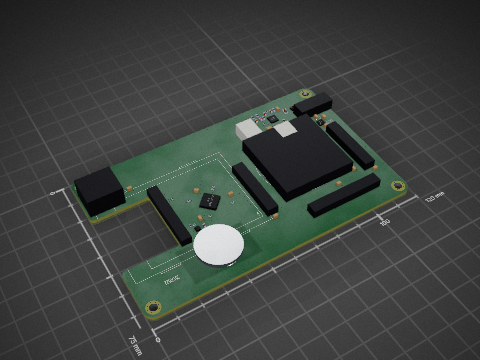

bfarago/xmos_cpld_slice
This is a slice extender panel, which contains a small cpld, aimed to have configurable the bridge between the slot and the slice panel.


hackclub/OnBoard
💡 Join 1,000 teenagers and make your first PCB with a $100 grant!

Chrismettal/EleLab_v2
Cheap DIY lab system for hobbyists and the tinkering folk

Chrismettal/flipper-zero-backpacks
Backpack-style addon boards for the Flipper Zero!
It measures 96.5 × 96.5 mm and has 2 copper layers, 1.6 mm thick.
40 parts, built around the 5M160ZT100C5N, 5M240ZT144C5N and 5M40ZE64C5N. The full list of its parts is on this page, with links to each part's symbol and footprint where PCBKit's library has them.
From the emtenet/max-v-fuse-map repository on GitHub, at the commit this page was made from: the board is dev-board/dev-board.kicad_pcb and its schematic dev-board/E64.kicad_sch. PCBKit opens the board in the browser, with nothing to install.
Its repository publishes it under the ISC licence: you may reuse it on that licence's terms (keep the author's notice, and for a copyleft licence share your changes alike).