2 layers428 × 293 mm

 emperor-hadrian/stack_machine
Design for a DIY computer
Control unit central timing is an open-source printed circuit board by emperor-hadrian, from the emperor-hadrian/stack_machine repository on GitHub. It is a 2-layer board of 100 × 100 mm with 25 parts on 91 nets, routed with 939 tracks and 93 vias.
Its parts include 23 ICs and 2 resistors.
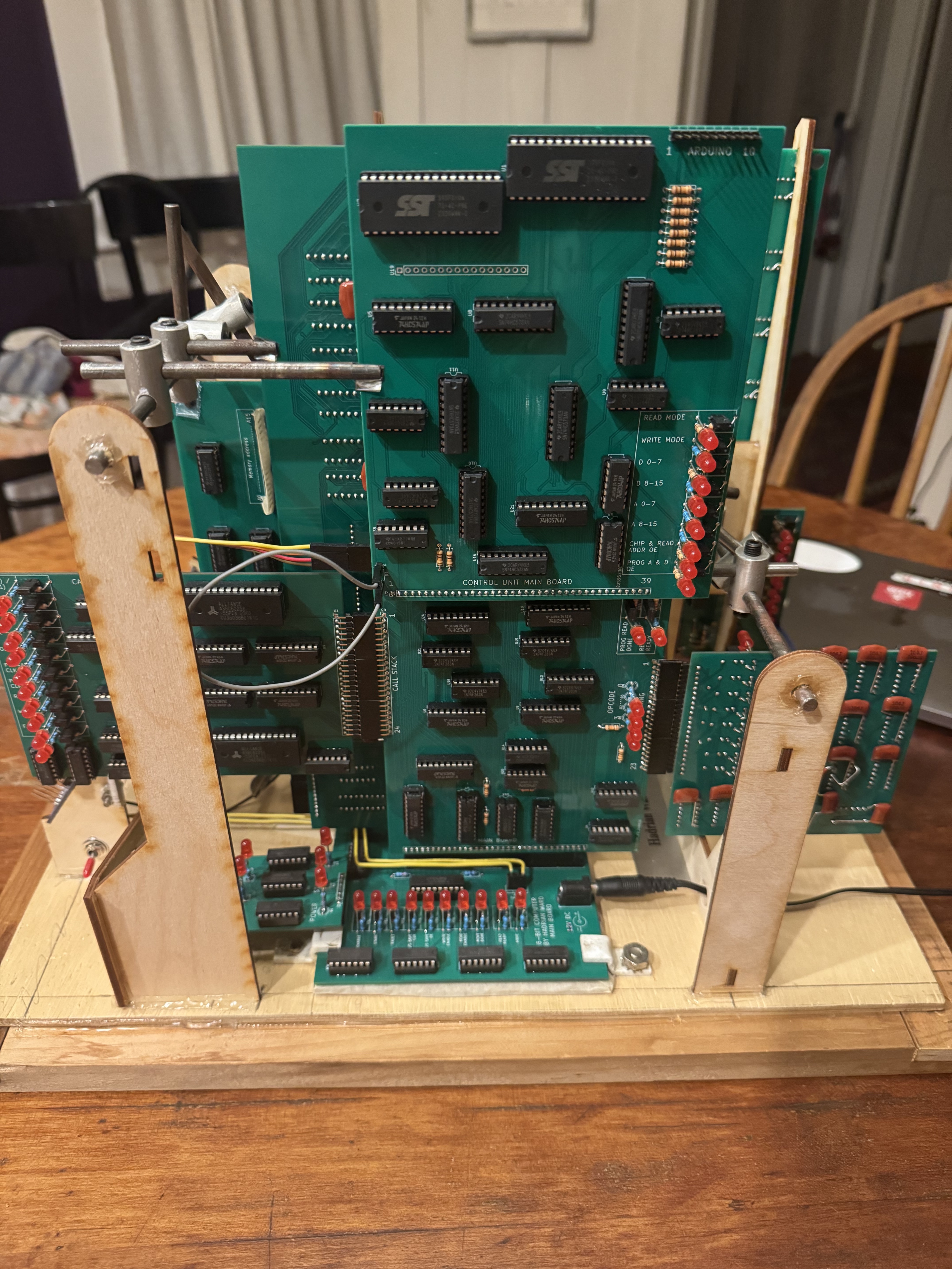
Photo of Version 1
(prog_addr - 32,768) * 2. Since that will only happen at or above 32,768 then the MSB will not be used in the math and will be used to determine whether to read from flash or GPRAM.The RAM chips have 15 address lines each so there will be two of them (Lower and Upper Domains). This means that they can be used seperately at the same time, for example fetching the new instruction (If the PC is in the RAM) and also doing GPRAM read/write, as long as these operations are using seperate domains. Memory users will use either (or both) of the lower or upper RAM domains:
Each instruction will be 16 bits and interpreted by the control unit. The first 4 bits (0 - 3) of the instruction will address the below list of operations. The rest of the instruction (bits 4 - 15) may be ignored or used for different things depending on the specific operation.
Here's the current list of the operation codes (opcodes):
MOVE - Bus usage - The rest of the instruction will be interpreted as follows: bits 8 - 11 address the device which will set the state of the bus (TX) and bits 12 - 15 will address the device to read from it (RX). Bits 4 - 7 are sent to the ALU as it's opcode incase the data is comming from it.WRITE - Writes instruction bits 4 - 11 to the bus. Bits 12 - 15 address the device to read from it.GOTO - Saves the 2 execution pointer GOTO latches (each of them are 1 byte) to the program counterGOTO-IF - Reads the LSB of the value in the goto decider latch and does a GOTO only if it is 1, otherwise does nothingHALT - Stops the clock, usefull for debuggingCALL - Effectively the same as GOTO but also pushes the return address (current value of program counter) onto the call stack. Note: The return address can be copied as-is and does not need to be incremented because it will be incremented normally after each RETURN instruction when it is used. If bit 4 is 1 this means that this call is calling the interrupt handler using the Interrupt GOTO latches.RETURN - The program counter will be set to the return address popped off the top of the call stack. If bit 4 is 1 this means that this return instruction is returning from the interrupt handler function and will allow interrupts again.CONFIG-INT - Configure interrupt. Bit 4 enables or disables interrupts. Interrupts are disabled on startup.The following are treated as either MOVE or WRITE by the sequencer and set the bus TX and RX MSBs. The original MOVE and WRITE have all MSBs = 0.
MOVE - MSBs TX=1, RX=0MOVE - MSBs TX=0, RX=1MOVE - MSBs TX=1, RX=1WRITE - MSBs RX=1Up to 15 devices can read the bus and 16 write to it. Devices that can read the bus (RX):
NONE - Nothing reads this so that bytes can be popped from the stack without them going anywhere.STACK-PUSH - Stack controller (Push)ALU-A - ALU latch AALU-B - ALU latch BGOTO-A - Control unit - Program counter GOTO latch A (first byte)GOTO-B - Control unit - Program counter GOTO latch B (second byte)GOTO-DECIDER - Control unit - GOTO decider latch (For GOTO-IF)GPRAM - GPRAM - WriteGPRAM-INC-ADDR - GPRAM - Write (++ address)GPRAM-ADDR-A - GPRAM - Address bits 0 - 7GPRAM-ADDR-B - GPRAM - Address bits 8 - 15GPIO-WRITE-A - Writes to GPIO output pins 0 - 7OFFSET-WRITE - Replaces value in stack at ToS - offsetSET-STACK-OFFSET - Sets the stack offset byteALU-C-IN - ALU latch for carry and borrow, only LSB is used. Make sure this is always zero when not being used otherwise additions will be wrong.GPIO-WRITE-B - Writes to GPIO output pins 8 - 15INT-GOTO-A - Interrupt GOTO AINT-GOTO-B - Interrupt GOTO BVECTORS-A - Vector graphics A inputVECTORS-B - Vector graphics B inputVECTORS-C - Vector graphics C inputVECTORS-D - Vector graphics D inputINT-AND-MAIN-TIMER-ADDRESS - Bits 0 - 1 address 1 of the 4 interrupt timers. Bit 2 will reset the addressed counter to 0.INT-TIMER-CONFIG-MAX - Sets the start value of one of the interrupt timersINT-TIMER-CONFIG-TIMEBASE-AND-ENABLE - Configures one of the interrupt timers, see timer_board.mdFLASH - Flash programming interface, same as the arduino connectionRX-26 - Expansion RX 25...
RX-31 - Expansion RX 31Devices that can write to the bus (TX):
STACK-POP - Stack controller (pop)OFFSET-READ - Reads value from stack at ToS - offset, does not affect the ToSALU - ALU outputWRITE instructionGPRAM - GPRAM - ReadGPRAM-INC-ADDR - GPRAM - Read (++ address)GPRAM-ADDR-A - GPRAM - Address bits 0 - 7GPRAM-ADDR-B - GPRAM - Address bits 8 - 15GPIO-READ-A - Reads GPIO input pins 0 - 7MAIN-TIMER - 8 bits of the main timer, addressed by INT-AND-MAIN-TIMER-ADDRESSINT-TIMER - Current value of 1 of the 4 interrupt timers, addressed by INT-AND-MAIN-TIMER-ADDRESSGPIO-READ-B - Reads GPIO input pins 8 - 15INT-CODE - Most recent interrupt code, will be cleared upon readINT-COUNT - Number of interrupts in queue, will overflow past 255GET-STACK-OFFSET - Retrieves stack offset, needed to save state during interruptGET-GOTO-A - Read GOTO Latch AGET-GOTO-B - Read GOTO Latch BTX-17 - Expansion TX 17...
TX-31 - Expansion TX 31The stack will simply be a piece of memory seperate from the GPRAM and managed by hardware, its has 32k x 8-bit words.
There will be two ways to access the stack:
OFFSET-WRITE and OFFSET-READ) (does not change ToS). The stack offset will be a 1-byte number set from the bus (SET-STACK-OFFSET) and will not affect pushes and pops.The ALU uses 2 8-bit latches for input and has 1 output. The specific operation it does is controlled by 4 bits (2^4 = 16 operations). All operations that result in a boolean output all 0s except for the result which is the LSB.
ADD - AddADD-C - Addition carry output (just the LSB will be set), this can be written directly into ALU-C-INNOT - Bitwise NOT (latch A)OR - Bitwise ORAND - Bitwise ANDXNOR - Bitwise XNOR, whether each pair of bits are equalSHIFT - Bitshifts A left by the first 3 bits of B, bits that go off the end DO wrap around.EQ - Whether bytes are equalA - Contents of A latchB - Contents of B latchEXT-10 - Extension (not implemented)EXT-11 - Extension (not implemented)EXT-12 - Extension (not implemented)EXT-13 - Extension (not implemented)EXT-14 - Extension (not implemented)EXT-15 - Extension (not implemented)There are four instructions for flow control: GOTO, GOTO-IF, CALL, and RETURN.
A GOTO instruction is used to jump to anywhere in the program. it uses the two 8-bit latches (GOTO-A and GOTO-B) to set the 16-bit program counter. Due to how the hardware is set up, the PC will be incremented after each goto instruction. This means that the previous address to where the execution should jump to must be used.
GOTO-IF is a conditional goto which will do what is described above only if the bit set by GOTO-DECIDER from the LSB of the bus is 1, otherwise it does nothing. This is the only instruction that allows the computer to "branch" or "make decisions".
There are macros, @goto(anchor_name) and @goto_if(anchor_name) that make GOTOs a lot easier.
Functions in the machine code are defined by CALL and RETURN instructions. To call a function, make sure the correct pointer to the beginning of the function is stored in the control unit goto A and B latches. Then use the CALL instruction which is basically a GOTO but will first put the current program counter value onto the call stack as the return address. The return instruction pops a return address off of the call stack and continues execution.
There is a macro in the assembly language, @call(function_name) that makes calling a lot easier.
The call stack is a seperate stack memory containing 256 (1 byte address size) 16-bit words. Each word will be a return address - where to set the program counter during a RETURN instruction.
There are 16 input and 16 seperate output pins accessible with the GPIO-READ-A, -B and GPIO-WRITE-A, -B bus sources/destinations.
The display has 32 x 32 LEDs, any given row of 8 pixels are written all at once with one byte. These rows of 8 are addressed by a 7-bit number starting at the top-left and going across for 4 per row (32 / 8 = 4) for each of the 32 rows of the display. The display currently is attached to the gpio-write a and b outputs with gpio-write-a being the address (MSB is ignored) and gpio-write-b being the data. The signal to write the address/data to the display's memory is sent by the hardware when gpio-write-b is written to, meaning the address should be written first and then the data.
This piece of memory does not have any hardware protection like the stack and can be writen to and read from at any location. It will have a 16-bit address by 8-bit word size (65,536 bytes) just like the stack.
Its address can be optionally incremented upon reads/writes and can be directly set from the bus (GPRAM-ADDR-A and GPRAM-ADDR-B). For the instructions where the address is incremented, that will happen after the read/write.
First, everything was built and tested in a digital circuit simulator Rusty Logic which allowed my to check that all the timing diagrams would be followed.
Once everything was working in Rusty Logic, KiCad was used to layout all of the actual PCBs.
| Qty | Value | Footprint | References |
|---|---|---|---|
| 11 | ~ | Package_DIP:DIP-14_W7.62mm | U2, U4, U5, U9, U10, U11, U12, U13, U14, U15, U16 |
| 8 | ~ | custom_footprint_library:jumper | U6, U17, U18, U19, U20, U21, U22, U23 |
| 2 | 10k | custom_footprint_library:0.4_pitch_resistor | R1, R2 |
| 2 | ~ | Package_DIP:DIP-20_W7.62mm | U7, U8 |
| 1 | ~ | Package_DIP:DIP-16_W7.62mm | U3 |
| 1 | ~ | Connector_PinHeader_2.54mm:PinHeader_1x23_P2.54mm_Horizontal | U1 |
It measures 100 × 100 mm and has 2 copper layers, 1.6 mm thick.
25 parts. The full list of its parts is on this page, with links to each part's symbol and footprint where PCBKit's library has them.
From the emperor-hadrian/stack_machine repository on GitHub, at the commit this page was made from: the board is kicad/boards_version_1/control_unit_central_timing/control_unit_central_timing.kicad_pcb. PCBKit opens the board in the browser, with nothing to install.
Its repository states no licence, so its author keeps all rights: ask emperor-hadrian before reusing the design.


google/mozc-devices
Circuit diagrams and firmware source code for Gboard DIY keyboards

davidphilipbarr/Sweep
Sweep - a small promicro based keyboard inspired by the Ferris.


hackclub/OnBoard
💡 Join 1,000 teenagers and make your first PCB with a $100 grant!

xyphro/UsbGpib
Versatile, cheap and portable USB to GPIB converter (USBTMC class based)


jes/scamp-cpu
A homebrew 16-bit CPU with a homebrew Unix-like-ish operating system.
