
2 layers139.7 × 41.9 mm
Kstat mainboard
nfroehberg/GlazerLab_KStat
Firmware, PCB design and Python interface for the KStat potentiostat developed in the Glazer Lab, University of Hawaii.
121 parts
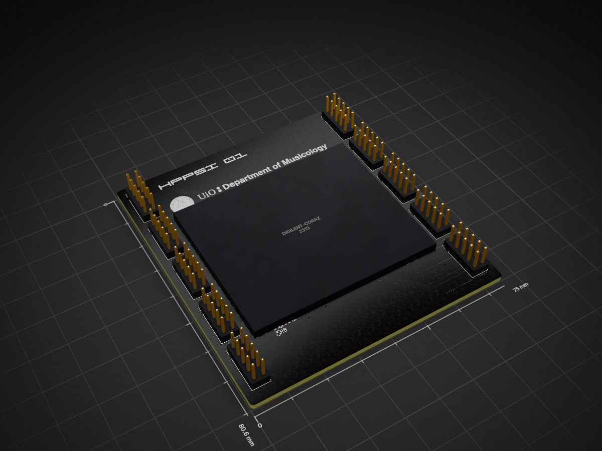
 emoninet2/HPPSI01
HPPSI01 is an open-source printed circuit board by emoninet2, from the emoninet2/HPPSI01 repository on GitHub. It is a 2-layer board of 75 × 80.6 mm with 43 parts on 165 nets, routed with 1,332 tracks and 63 vias.
It is built around the MAX4617EUE+. Its parts include 16 resistors, 11 ICs, 10 connectors and 4 capacitors.
| Qty | Value | Footprint | References |
|---|---|---|---|
| 10 | Conn_02x05_Odd_Even | Connector_PinHeader_2.54mm:PinHeader_2x05_P2.54mm_Vertical | J1, J2, J3, J4, J5, J6, J7, J8, J9, J10 |
| 10 | MAX4617EUE+ | Package_SO:TSSOP-16_4.4x5mm_P0.65mm | U1, U2, U3, U4, U5, U6, U7, U8, U9, U10 |
| 4 | 140 | Resistor_SMD:R_0402_1005Metric | R1, R3, R5, R7 |
| 4 | 1K | Resistor_SMD:R_0402_1005Metric | R10, R12, R14, R16 |
| 4 | 1nF | Capacitor_SMD:C_0402_1005Metric | C1, C2, C3, C4 |
| 4 | 2.32K | Resistor_SMD:R_0402_1005Metric | R9, R11, R13, R15 |
| 4 | 845 | Resistor_SMD:R_0402_1005Metric | R2, R4, R6, R8 |
| 1 | Digilent-CoraZ7_units | footprint:CoraZ7_stack | U11 |
| 1 | LOGO | footprint:HPPSI_02_logo | G*** |
| 1 | LOGO | footprint:UiO_DoM | G*** |
It measures 75 × 80.6 mm and has 2 copper layers, 1.6 mm thick.
43 parts, built around the MAX4617EUE+. The full list of its parts is on this page, with links to each part's symbol and footprint where PCBKit's library has them.
From the emoninet2/HPPSI01 repository on GitHub, at the commit this page was made from: the board is Board/HPPSI01.kicad_pcb. PCBKit opens the board in the browser, with nothing to install.
Its repository states no licence, so its author keeps all rights: ask emoninet2 before reusing the design.
nfroehberg/GlazerLab_KStat
Firmware, PCB design and Python interface for the KStat potentiostat developed in the Glazer Lab, University of Hawaii.

shraken/usbhid_buddy
Hardware, firmware, and software for the USBHID DAQ 'Buddy' device

google/mozc-devices
Circuit diagrams and firmware source code for Gboard DIY keyboards

rusefi/rusefi
rusefi - GPL internal combustion engine control unit


jrsteensen/OpenHornet
OpenHornet 1:1 F/A-18C Simulator Repository


tebl/RC6502-Apple-1-Replica
An expandable SBC-version of the Apple 1 computer, easy to get started with and lot of cool stuff that can be added to it!