GNN-guided simulated annealing for PCB component placement. We train a Graph Attention Network on SA rollout data to learn which components to move and where, then use these predictions to bias the SA search.
Rp2040 debugger is an open-source printed circuit board by elcruzo, from the elcruzo/learned-pcb-placement repository on GitHub, published under the MIT licence. It is a 4-layer board of 57 × 47.5 mm with 69 parts on 64 nets, routed with 560 tracks and 87 vias.
It is built around the RP2040, W25Q16JVSSIQ and TLV1117LV33DCYR, with the LTST-C150KRKT among its other parts. Its parts include 21 capacitors, 17 resistors, 10 connectors, 5 diodes and 4 ICs. It belongs with the interfaces and adapters boards and the RP2040 boards of this library.
GNN-guided simulated annealing for PCB component placement. We train a Graph Attention Network on SA rollout data to learn which components to move and where, then use these predictions to bias the SA search. Early results show up to 9.2% HPWL reduction on KiCad designs. Dataset includes production boards up to 681 components (Antmicro Jetson Orin baseboard, HackRF One SDR).
KiCad .kicad_pcb
     │
     ▼
┌──────────────┐
│  S-expr Parser │ ──→ Components, Nets, Board geometry
└──────┬───────┘
       │
       ▼
┌──────────────┐     ┌──────────────┐
│  Graph Laplacian │ ──→ │ Spectral Init │ (Fiedler vectors)
│  L = D - A       │     └──────┬───────┘
└──────────────┘              │
       │                      ▼
       ▼             ┌──────────────┐
┌──────────────┐     │   SA Rollouts  │ ──→ Training data
│  GAT (2-layer)  │◀──  │  10 × short SA │     (accepted moves,
│  4-head attn    │     └──────────────┘      improvements)
│  move + quality │
└──────┬───────┘
       │
       ▼
┌──────────────────────────┐
│  GNN-Guided SA              │
│  P(component i) ∝ softmax(q_i / τ)  │
Results
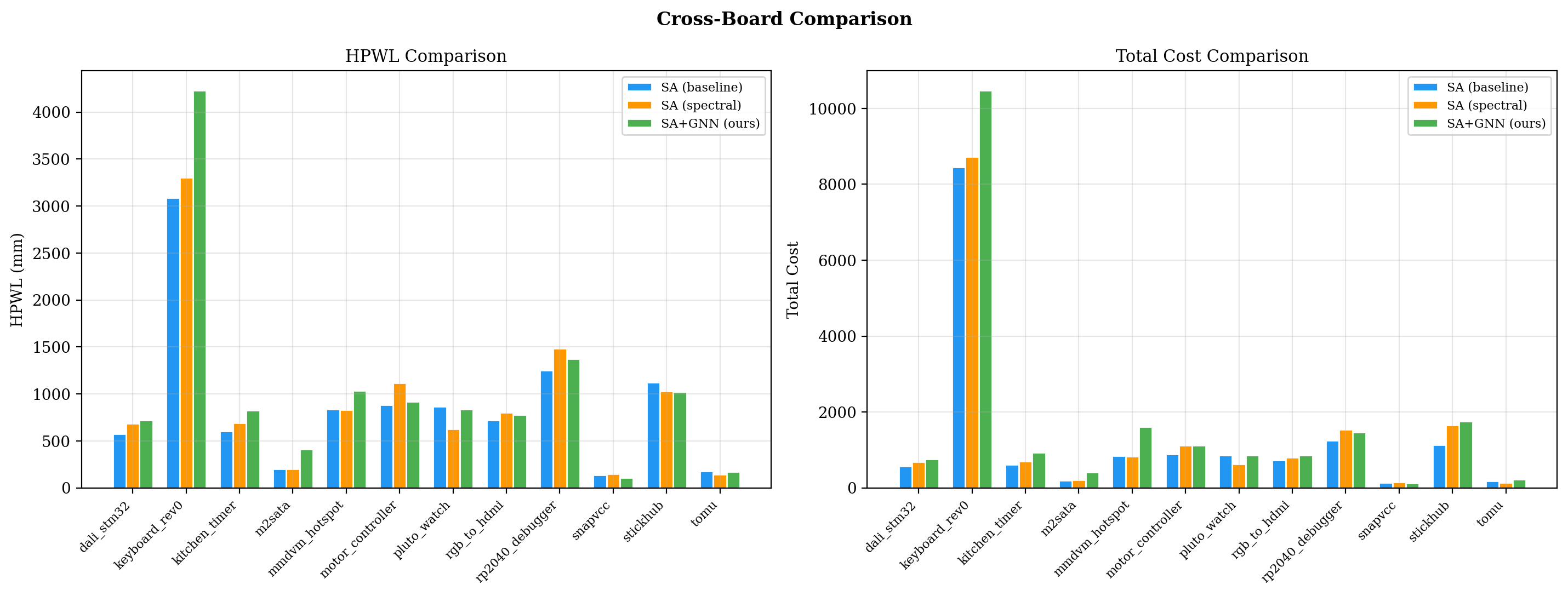
Evaluated on 12 KiCad PCBs (5 to 94 components) parsed directly from .kicad_pcb files, sourced from open-source hardware on GitHub. Three additional production boards (207 to 681 components) are included in the dataset for GPU/TPU evaluation via Colab.
Board
Components
Nets
SA HPWL
GNN HPWL
HPWL Δ
SA Cost
GNN Cost
stickhub
94
45
1125.9
1022.1
-9.2%
1127.8
1757.3
rp2040_debugger
69
55
1248.8
1375.4
+10.1%
1251.1
1464.6
motor_controller
51
36
883.2
918.4
+4.0%
883.5
1116.6
keyboard_rev0
37
46
3086.2
4228.8
+37.0%
8459.2
10468.6
pluto_watch
37
52
867.1
838.0
-3.4%
867.2
862.0
kitchen_timer
35
31
605.9
828.4
+36.7%
611.1
935.4
rgb_to_hdmi
32
32
721.9
776.8
+7.6%
723.5
865.7
snapvcc
26
8
136.4
106.9
-21.6%
136.5
118.2
dali_stm32
22
33
572.5
721.0
+25.9%
572.5
760.6
mmdvm_hotspot
21
29
839.7
1033.5
+23.1%
840.0
1606.8
tomu
17
17
176.5
174.1
-1.4%
176.5
222.7
m2sata
5
17
200.1
410.9
+105.3%
200.1
411.7
Key findings:
GNN achieves lower HPWL on 4 out of 12 boards (stickhub -9.2%, snapvcc -21.6%, pluto_watch -3.4%, tomu -1.4%)
On snapvcc (26 components), GNN also wins on total cost (118.2 vs 136.5), with overlap penalty of only 1.13
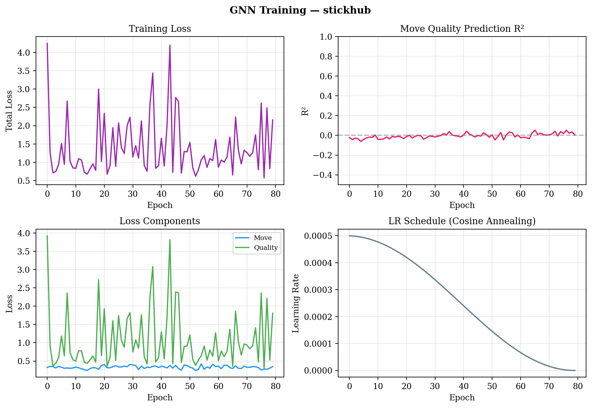
Overlap remains the primary bottleneck — the quality prediction head R² is low across all boards
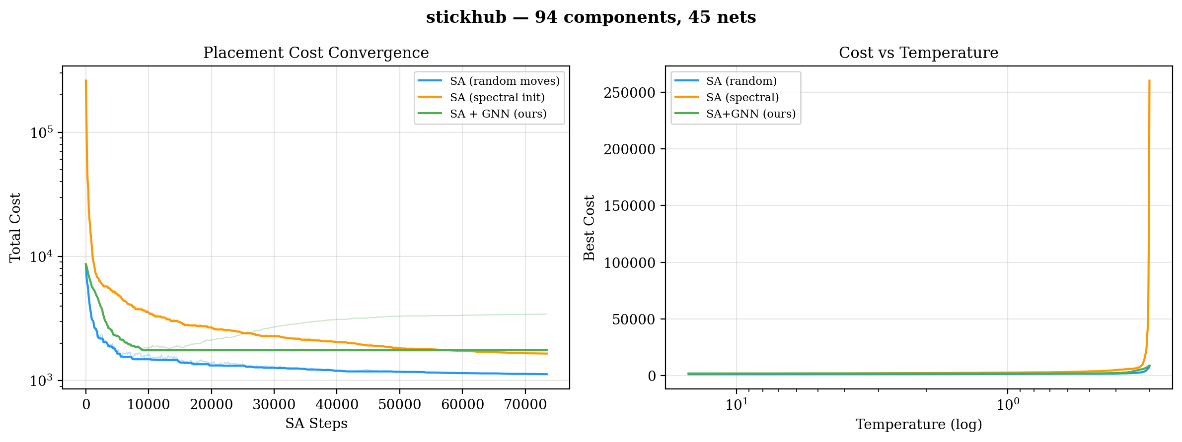
GNN acceptance rates are consistently higher (80-99%) vs baseline SA (50-93%), confirming the network proposes structurally meaningful moves
Per-board training with just 10 SA rollouts (~3-20s) — no pre-training, no large dataset
Quick Start
bash
pip install torch numpy matplotlib
python3 learn.py data/stickhub.kicad_pcb       # single board, default (80 epochs, 10 rollouts)
python3 graphs.py                                # generates all plots from results/
Or run scaled experiments on Google Colab (50 rollouts, 200 epochs, GPU/TPU):
Requires Python 3.10+ and PyTorch with CUDA, TPU (via torch_xla), MPS (Apple Silicon), or CPU fallback.
Data
15 KiCad PCB designs from open-source hardware, spanning hobby projects to production carrier boards:
GAT architecture, training loop, GNN-guided SA, experiment runner
placer.py
KiCad parser, cost functions, baseline SA, spectral placement
graphs.py
Publication-quality matplotlib plots
program.md
Experiment strategy and research plan
Why PCB Placement is Hard
PCB placement is NP-hard. A board with N components and G grid positions has O(G^N) configurations. The optimization landscape includes wirelength, component overlap, board boundary constraints, EMC, thermal, and signal integrity — all interacting across domains.
SA has been the gold standard for 40 years because the Boltzmann acceptance criterion (P = e^{-ΔE/T}) allows escaping local minima. But SA relies on random move proposals. Our insight: a GNN trained on short SA rollouts can learn which components to move and in which direction, replacing random exploration with informed proposals.
Related Work
All serious placement research targets VLSI/ASIC. PCB placement is wide open.
HPWL (wirelength) — total half-perimeter wirelength across all nets. Shorter wires mean easier routing, lower resistance, and less parasitic inductance.
Overlap penalty — components must not physically intersect. Penalized quadratically.
Boundary penalty — all components must stay within the board outline.
These are the standard baseline metrics for placement research (VLSI uses the same starting point). The system does not yet model:
Decoupling capacitor proximity — bypass caps must sit within a few mm of their IC's power pins. The netlist already encodes this relationship (cap and IC share a power net), so the GNN graph contains the signal — it just isn't weighted yet.
Functional group clustering — power regulation, analog front-end, digital core, and I/O should form coherent groups. Today the placer treats all components equally.
EMI/EMC separation — noisy switching regulators should be far from sensitive analog inputs. High-speed clock traces should be short and shielded. Not modeled.
Signal integrity — matched-length differential pairs, controlled impedance, return path continuity. Not modeled.
Thermal constraints — power components need spacing and copper pour area for heat dissipation. Not modeled.
The roadmap is to add these as weighted terms in the cost function (e.g., cost = HPWL + overlap + decoupling_distance + group_separation + EMI_penalty) and encode constraint types as edge features in the GNN graph so the network learns that some connections (power net between cap and IC) matter more than others (signal net between distant connectors).
What's Next
The GNN learns wirelength optimization but underfits on quality prediction (R² ≈ 0.001–0.079), which is why overlap isn't resolved. The local runs used only 10 rollouts and 80 epochs — not enough signal. The path forward:
Scale training on Colab — 50 rollouts, 200 epochs on GPU/TPU. 5x more data should address underfitting on the quality head.
Overlap-aware loss — penalize overlap in the GNN training objective, not just in the SA cost function.
Cross-board pre-training — train a single model on all 12 boards jointly, evaluate transfer to unseen designs.
Constraint-aware cost function — add decoupling cap proximity, functional group clustering, and EMI separation penalties. Encode net types (power, signal, clock) as edge features so the GNN learns constraint priorities.
Longer rollouts — current rollouts are short (T: 10→2). Longer annealing gives the GNN better examples of overlap resolution.
Diffusion hybrid — use a diffusion model for initial placement, then GNN-guided SA for refinement.
GNN-guided simulated annealing for PCB component placement. We train a Graph Attention Network on SA rollout data to learn which components to move and where, then use these predictions to bias the SA search.
GNN-guided simulated annealing for PCB component placement. We train a Graph Attention Network on SA rollout data to learn which components to move and where, then use these predictions to bias the SA search.
GNN-guided simulated annealing for PCB component placement. We train a Graph Attention Network on SA rollout data to learn which components to move and where, then use these predictions to bias the SA search.
PCB hardware designs in KICAD for Acorn, the precision farming rover from Twisted Fields.
198 parts81
Questions
How big is the Rp2040 debugger PCB?
It measures 57 × 47.5 mm and has 4 copper layers, 1.6 mm thick.
What parts does the Rp2040 debugger use?
69 parts, built around the RP2040, W25Q16JVSSIQ, TLV1117LV33DCYR and LTST-C150KRKT. The full list of its parts is on this page, with links to each part's symbol and footprint where PCBKit's library has them.
Where can I download the Rp2040 debugger KiCad files?
From the elcruzo/learned-pcb-placement repository on GitHub, at the commit this page was made from: the board is data/rp2040_debugger.kicad_pcb. PCBKit opens the board in the browser, with nothing to install.
Can I use the Rp2040 debugger design in my own project?
Its repository publishes it under the MIT licence: you may reuse it on that licence's terms (keep the author's notice, and for a copyleft licence share your changes alike).