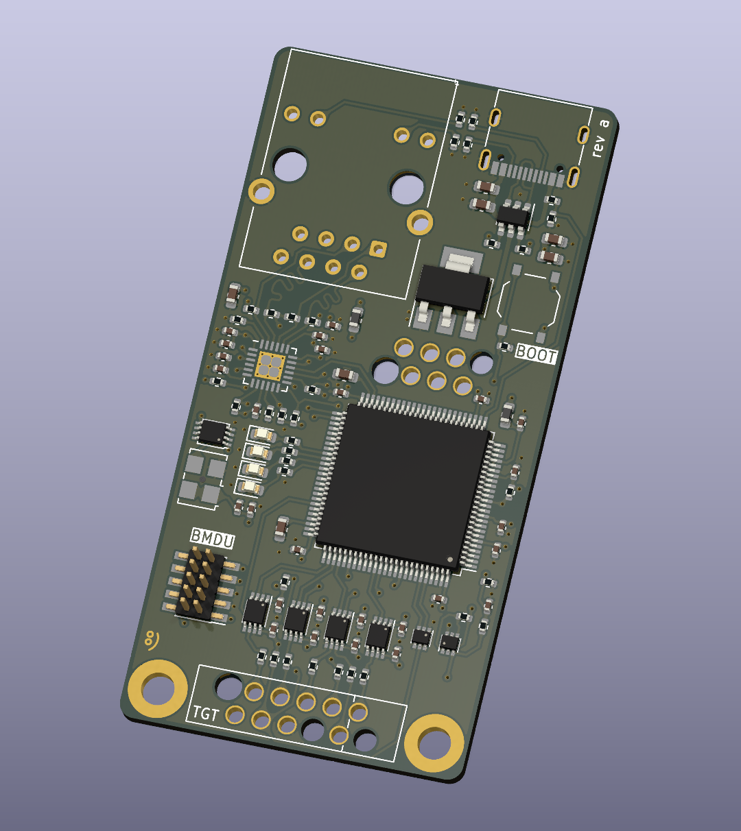
4 layers33.5 × 66.8 mm
Net bmp
elagil/net-bmp
An Ethernet-connected SWD/JTAG debug adapter (blackmagic probe)
97 parts3GPL-3.0

 elagil/net-bmp3
An Ethernet-connected SWD/JTAG debug adapter (blackmagic probe)
Debug adapter is an open-source printed circuit board by elagil, from the elagil/net-bmp repository on GitHub, published under the GPL-3.0 licence. It is a 2-layer board of 33.5 × 17.8 mm with 6 parts on 9 nets, routed with 31 tracks and 4 vias.
It belongs with the interfaces and adapters and sensors and measurement boards of this library.
| Qty | Value | Footprint | References |
|---|---|---|---|
| 2 | MountingHole | MountingHole:MountingHole_3.2mm_M3_ISO7380_Pad | H1, H2 |
| 1 | BMDU | Connector_PinSocket_1.27mm:PinSocket_2x05_P1.27mm_Vertical_SMD | J3 |
| 1 | Logo_Open_Hardware_Large | Symbol:OSHW-Symbol_6.7x6mm_SilkScreen | oshw1 |
| 1 | TC2030 | Connector_IDC:IDC-Header_2x03_P2.54mm_Vertical | J1 |
| 1 | UART | Connector_PinHeader_2.54mm:PinHeader_1x03_P2.54mm_Vertical | J2 |
elagil/net-bmp
An Ethernet-connected SWD/JTAG debug adapter (blackmagic probe)

byrantech/laptop
anyon_e, a highly integrated, high end, open source laptop. Attempt the impossible.


Jcparkyn/dpoint
Open-source digital stylus using camera tracking and inertial measurements

VoronDesign/Voron-Hardware
Cool Hardware designed by the Voron Design group

hoglet67/RGBtoHDMI
Bare-metal Raspberry Pi project that provides pixel-perfect sampling of Retro Computer RGB/YUV video and conversion to HDMI

hackclub/OnBoard
💡 Join 1,000 teenagers and make your first PCB with a $100 grant!

Luos-io/luos_engine
Open-source and real-time orchestrator for cyber-physical-systems, to easily design, test and deploy embedded applications and digital twins.

It measures 33.5 × 17.8 mm and has 2 copper layers, 1.6 mm thick.
6 parts. The full list of its parts is on this page, with links to each part's symbol and footprint where PCBKit's library has them.
From the elagil/net-bmp repository on GitHub, at the commit this page was made from: the board is hardware/adapter/debug_adapter.kicad_pcb and its schematic hardware/adapter/debug_adapter.kicad_sch. PCBKit opens the board in the browser, with nothing to install.
Its repository publishes it under the GPL-3.0 licence: you may reuse it on that licence's terms (keep the author's notice, and for a copyleft licence share your changes alike).