


2 layers52 × 89.5 mm
RP2350B RM2
eelstretching/rp2350b-rm2-reference
Raspberry Pi's RP2350B minimal design (RPI-RP2350B-MINIMAL R4-S1, KiCad 10) with these additions:
57 parts

 eelstretching/led-processor-board
A board with a processor and a couple of other things that can talk to an LED output board.
Led processor board is an open-source printed circuit board by eelstretching, from the eelstretching/led-processor-board repository on GitHub. It is a 2-layer board of 100 × 89.5 mm with 128 parts on 131 nets, routed with 1,126 tracks and 212 vias.
It is built around the RP2350B, W25Q128JVSIQ and APS6404L-3SQR-SN, with the DS3231SN#T&R, TPS54202HDDC and B5819W among its other parts. Its parts include 54 resistors, 42 capacitors, 9 connectors, 7 ICs and 5 diodes. It belongs with the RP2350 boards of this library.


The brains for the LED output boards: an RP2350B with an RM2 radio, 8 MB PSRAM, a DS3231 RTC and four 16-pin ribbon shrouds. Each shroud drives one led-output-board, which does the level shifting, fusing and strand connectors, so this board carries no LED power.
The core (RP2350B, flash, PSRAM, RM2, crystal, BOOTSEL/RUN buttons, 3.3 V regulator) is the rp2350b-rm2-reference schematic unchanged, except that its micro-B USB is now USB-C. That board's single-row J2/J3 headers are gone; the rest is new.
Status: schematic and first layout done, not yet built. ERC is clean apart from the four items inherited from Pi's design, and DRC has no copper errors and nothing unconnected (see "Verification").
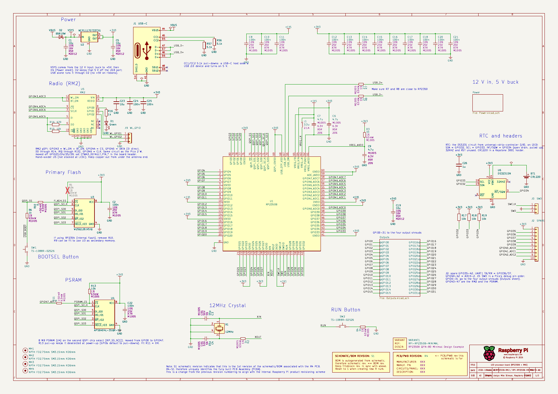
All three sheets: docs/schematic.pdf (Power, Outputs).
| GPIO | Use |
|---|---|
| 0-7 | OUT1 (J5) data 1-8 |
| 8-15 | OUT2 (J6) data 1-8 |
| 16-23 | OUT3 (J7) data 1-8 |
| 24-31 | OUT4 (J8) data 1-8 |
| 32 | RTC SDA (I2C0), 10k pull-up |
| 33 | RTC SCL (I2C0), 10k pull-up |
| 34 | RTC INT/SQW, 10k pull-up (open drain) |
| 35-42 | J2 spare header (UART1 TX/RX on 36/37; 40-42 are ADC0-2) |
| 43-46 | RM2 (WL_ON + BT_ON, CS, DATA, CLK), as on the reference board |
| 47 | PSRAM chip select, as on the reference board |
All 32 outputs sit in GPIO 0-31, so one PIO block (GPIO base 0) reaches every output. The radio's
PIO uses the 16-47 window, so it has to be a different PIO block from the LED renderer's. The
board header is firmware/boards/led_processor_board.h (the reference board's rp2350b_rm2.h
plus the RTC pins); see firmware/README.md for the DS3231 driver and the
rtc_set firmware.
The same pinout as the output boards' J2 (and MegaTree docs/power.md). Pin 1 is the triangle on
the shroud.
| Pin | Signal | Pin | Signal |
|---|---|---|---|
| 1 | GND | 2 | data 1 |
| 3 | GND | 4 | data 2 |
| 5 | GND | 6 | data 3 |
| 7 | GND | 8 | data 4 |
| 9 | GND | 10 | data 5 |
| 11 | GND | 12 | data 6 |
| 13 | +3V3 (shifter VCCA) | 14 | data 7 |
| 15 | +5V (shifter VCCB) | 16 | data 8 |
Data n of OUTk is GPIO 8(k-1) + (n-1). Each data line has a 33R series resistor at the RP2350 end to damp ringing on the ribbon. Each shroud has 100n on +3V3 and on +5V.
J1 is a USB-C receptacle (Korean Hroparts TYPE-C-31-M-12, LCSC C165948, KiCad's stock
USB_C_Receptacle_HRO_TYPE-C-31-M-12 footprint) in place of Pi's micro-B. USB 2.0 only: D+ and D-
from both sides of the plug are joined, CC1 and CC2 each have a 5.1k pull-down (R56, R57) so a
USB-C charger or host turns on 5 V, SBU1/SBU2 are unconnected and the shell goes to GND. The
D+/D- nets (USB_D+/USB_D-, through Pi's 27R R7/R8) and VBUS into D2 are as before.
The DS3231 circuit from universal-strip-controller (its U9): DS3231SN, 1 uF on VCC, 10k pull-ups on SDA, SCL and INT/SQW, 32KHZ and RST unconnected. The coin cell is a CR1220 in a Keystone 3001 holder, so it can be replaced (universal-strip-controller used a tabbed cell).
cyw43_arch_gpio_put() /
cyw43_arch_gpio_get(), which go over the radio's SPI link, so they're slow, plain digital in/out
(no PWM, PIO or ADC). Fine for an LED, a button or a relay in a pinch. On a Pico 2 W these two are
SMPS mode and VBUS sense; here nothing else uses them.production/ holds the BOMs and the JLCPCB upload set. bom-full.csv is the full BOM with LCSC
numbers (edit this one); the rest is made from it and the board by
python3 tools/jlc.py (rerun it after any board change):
led-processor-board-gerbers.zip: gerbers and drill files.jlcpcb-bom.csv and jlcpcb-cpl.csv: BOM and placement for the 111 SMD parts JLC assembles
(everything on the top side with an LCSC number). JLC's 3D models don't always share KiCad's zero
angle: ROT_FIX in tools/jlc.py turns U2, U3, U4 and U6 a quarter turn to match (checked in
JLC's placement preview for the first order). Still check the preview: legs on pads, pink pin-1
dot at the board's pin-1 mark.tools/jlc.py needs KiCad's own Python (for pcbnew) and kicad-cli on the PATH. On a Mac with
KiCad in /Applications/KiCad, save the board in KiCad, then from the repo root:
K=/Applications/KiCad/KiCad.app/Contents
PATH=$K/MacOS:$PATH $K/Frameworks/Python.framework/Versions/Current/bin/python3 tools/jlc.py
git status production/   # see what changed, then commit and push
On Linux, with KiCad installed from its PPA, plain python3 tools/jlc.py works. The BOM and CPL
only change when parts move or the BOM changes; the gerbers zip changes with any copper or silk
edit.
Left off both files for hand-soldering:
SW1/SW2 are XKB TS-1088R-02526 (C455281, 4 x 3 mm) in place of Pi's Wurth 434133025816, which LCSC doesn't stock; same spots, same nets. R1 is DNP, as on the reference board. Pi's R9 (an unfitted 0R option from GPIO0 to the flash chip select) is removed, with its GPIO0 branch, so OUT1's first data line has no stub. The PSRAM chip select is GPIO47 (QMI CS1n, RP2350 datasheet section 9.4, which allows GPIO 0, 8, 19 or 47).
J4 (DORABO DB301V-3.5-2P, C695629) is in the same family as the output boards' strand terminals and uses KiCad's stock 3.5 mm Phoenix PT footprint; check the hole size against the DB301V drawing when laying out.
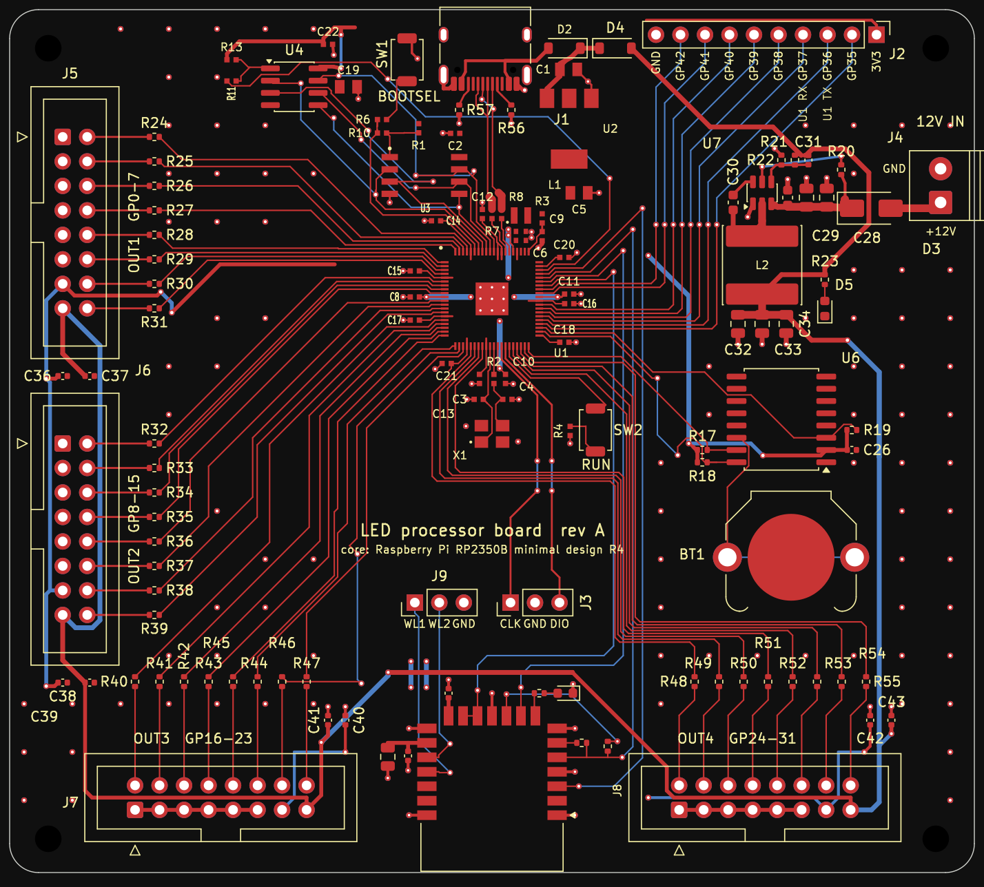
100 x 89.5 mm, 2 layers, four 2.75 mm (M2.5) mounting holes. 3D views: top, bottom; bottom copper: docs/pcb-bottom-copper.png.
The layout was built by scripts in tools/pcb/ (KiCad 10 Python API plus Freerouting 1.9.0). From
here on it is a normal KiCad board, so edit it in KiCad; the scripts are a record of how it was made.
build_pcb.py REF.kicad_pcb net.xml OUT.kicad_pcb . loads the reference layout, drops its
micro-B and headers, clips the routes that went to them, places the new parts
(placement.py) and hand-routes the power, USB-C, OUT4, RM2 and SWD runs (preroute.py).
net.xml is kicad-cli sch export netlist --format kicadxml.route.sh in out 20 exports a Specctra DSN, freezes the existing copper and sets net classes
(dsn_prep.py), runs Freerouting 1.9.0 (xvfb-run java -jar freerouting-1.9.0.jar; 2.x
ignores the pass limit and never writes the session), and imports the result.post.py trims dangling tails and adds GND stitching vias; fix.py adds the two +3V3 jumpers
under the +5V run to J7 and C40's link; rip.py plus a second route.sh rerouted the J2/RTC
fan-out (GPIO32-42), which the first pass left one net short on; silk.py places the reference
designators.psram.py (flip and place U4/C22/R11/R13, rip their bottom-side
routing), post.py --trim-only, psram2.py (Pi's QSPI escapes from under U3, the GPIO47 drop),
route.sh, then the U4 supply hop at the end of fix.py, post.py and silk.py.j2top.py (place it and its pin labels, rip its old fan-out),
post.py --trim-only, j2route.py (hand-routes the bus and moves the +3V3 hop from the core pour
to the RTC, which also feeds the lower pour and the RM2, below the via row), post.py, silk.py.shrouds.py (move J7/J8 and their caps, re-run the data
lines, rip their power), shrouds2.py (hand-routes their 3V3/5V), post.py, silk.py, then
hdrs.py (adds J9 and moves J3 under the board name), route.sh (WL_GPIO1/2), post.py,
silk.py, and swd.py (hand-routes SWCLK/SWD, which Freerouting couldn't get out of the core).buttons.py (TS-1088R footprints in SW1/SW2's spots, stubs re-joined) and
tools/sch_buttons.py (swaps the schematic symbols to Switch:SW_Push).tools/rm_r9.py drops R9 and its GPIO0 branch from the schematic and board; tidy_gpio.py
straightens GPIO0 and chamfers GPIO1 on their way to OUT1.render.sh / rendernz.sh make the PNGs (kicad-cli pcb export svg cropped with cairosvg;
rendernz hides zone fills).| Path | What |
|---|---|
led-processor-board.kicad_sch | root sheet: the reference core, RTC, J2/J3/J9, sheet symbols |
Power.kicad_sch | 12 V in, buck, +5V, VSYS |
Outputs.kicad_sch | J5-J8 shrouds, 33R series resistors, decoupling |
rp2350b_rm2.kicad_sym, rp2350b_rm2.pretty/ | RM2 symbol and footprint (from the reference) |
production/bom-full.csv | full BOM with LCSC numbers |
production/ (rest) | JLCPCB gerbers zip, assembly BOM and CPL (tools/jlc.py) |
docs/schematic.pdf, docs/sheet-*.png | all three sheets |
led-processor-board.kicad_pcb | the layout |
docs/pcb-*.png | layout previews |
tools/build_schematic.py | the one-off script that built these sheets from the reference (kept for reference; edit the schematic in KiCad from here on) |
tools/pcb/ | the scripts that built the layout (see "Regenerating it") |
kicad-cli sch erc (KiCad 10.0.7, stock libraries) reports the same four items as the reference
board, all in Pi's part of the design: U2's two OUT pins tied together, U1 VREG_AVDD and #PWR16
"not driven" (power-flag nits), and one off-grid wire end. The rest are notes that Pi's embedded
libraries (RPI_DB, RPI - Power, RPI_COMPILED) aren't in the library table, as on the
reference board. A netlist check confirms each shroud's GND, +3V3, +5V and data pins, the RTC nets
and the 12 V to VSYS chain.
kicad-cli pcb drc --severity-all --schematic-parity reports no clearance, short, hole or unconnected
items, and the board matches the schematic (apart from footprints not carrying the symbols'
manufacturer fields). What's
left: 41 warnings that Pi's RPI_COMPILED footprint library isn't in the library table (as on the
reference board), and 4 silkscreen-past-the-edge warnings from J1 and J4, whose bodies overhang the
board edge (the USB-C opening and the terminal block). C7 and C27 have their reference designators hidden
for lack of room.
Raspberry Pi's design is MIT (see LICENSE-RaspberryPi.txt); the additions here are MIT too.
| Qty | Value | Footprint | References |
|---|---|---|---|
| 32 | 33 | Resistor_SMD:R_0402_1005Metric | R24, R25, R26, R27, R28, R29, R30, R31, R32, R33, R34, R35, R36, R37, R38, R39 +16 |
| 14 | 100n | RPI_COMPILED:generic_capc1005x50 | C2, C8, C10, C11, C12, C13, C14, C15, C16, C17, C18, C20, C21, C22 |
| 10 | 100n | Capacitor_SMD:C_0402_1005Metric | C24, C25, C36, C37, C38, C39, C40, C41, C42, C43 |
| 4 | 10k | Resistor_SMD:R_0402_1005Metric | R15, R17, R18, R19 |
| 4 | NPTH FD2.75mm SM3.15mm KO6mm | RPI_COMPILED:none_mh_npth_fd2p75mm_sm3p15mm_ko6mm | MH1, MH2, MH3, MH4 |
| 3 | 10u | Capacitor_SMD:C_0805_2012Metric | C23, C27, C28 |
| 3 | 10u | RPI_COMPILED:generic_capc2012x125 | C1, C5, C19 |
| 3 | 1k | RPI_COMPILED:generic_resc1005x35 | R2, R4, R6 |
| 3 | 22u | Capacitor_SMD:C_0805_2012Metric | C32, C33, C34 |
| 2 | 0 | RPI_COMPILED:generic_resc1005x35 | R10, R11 |
| 2 | 100n | Capacitor_SMD:C_0603_1608Metric | C29, C30 |
| 2 | 10k | RPI_COMPILED:generic_resc1005x35 | R1, R13 |
| 2 | 15p | RPI_COMPILED:generic_capc1005x50 | C3, C4 |
| 2 | 1k | Resistor_SMD:R_0402_1005Metric | R16, R23 |
| 2 | 27 | RPI_COMPILED:generic_resc1005x35 | R7, R8 |
| 2 | 4.7u | RPI_COMPILED:generic_capc1005x50_wide | C6, C7 |
| 2 | 5.1k | Resistor_SMD:R_0402_1005Metric | R56, R57 |
| 2 | B5819W | Diode_SMD:D_SOD-123 | D2, D4 |
| 2 | Green | LED_SMD:LED_0603_1608Metric | D1, D5 |
| 2 | TS-1088R-02526 | Button_Switch_SMD:SW_SPST_TS-1088-xR025 | SW1, SW2 |
| 1 | 100k | Resistor_SMD:R_0402_1005Metric | R21 |
| 1 | 12MHz | RPI_COMPILED:generic_xtalcc320x250x80-4 | X1 |
| 1 | 12V IN | TerminalBlock_Phoenix:TerminalBlock_Phoenix_PT-1,5-2-3.5-H_1x02_P3.50mm_Horizontal | J4 |
| 1 | 13.3k | Resistor_SMD:R_0402_1005Metric | R22 |
| 1 | 15u | Inductor_SMD:L_Sunlord_SWPA8040S | L2 |
| 1 | 1u | Capacitor_SMD:C_0402_1005Metric | C26 |
| 1 | 3.3u | RPI_COMPILED:abracon_aota-b201610s3r3-101-t | L1 |
| 1 | 33 | RPI_COMPILED:generic_resc1005x35 | R3 |
| 1 | 4.7u | RPI_COMPILED:generic_capc1005x50 | C9 |
| 1 | 470 | Resistor_SMD:R_0402_1005Metric | R14 |
| 1 | 510k | Resistor_SMD:R_0402_1005Metric | R20 |
| 1 | 75p | Capacitor_SMD:C_0402_1005Metric | C31 |
| 1 | APS6404L-3SQR-SN | Package_SO:SOIC-8_3.9x4.9mm_P1.27mm | U4 |
| 1 | CR1220 | Battery:BatteryHolder_Keystone_3001_1x12mm | BT1 |
| 1 | DS3231SN | Package_SO:SOIC-16W_7.5x10.3mm_P1.27mm | U6 |
| 1 | NCP1117ST33T3G | RPI_COMPILED:onsemi_ncp1117st33t3g | U2 |
| 1 | OUT1 | Connector_IDC:IDC-Header_2x08_P2.54mm_Vertical | J5 |
| 1 | OUT2 | Connector_IDC:IDC-Header_2x08_P2.54mm_Vertical | J6 |
| 1 | OUT3 | Connector_IDC:IDC-Header_2x08_P2.54mm_Vertical | J7 |
| 1 | OUT4 | Connector_IDC:IDC-Header_2x08_P2.54mm_Vertical | J8 |
| 1 | RM2 | rp2350b_rm2:RPi_RM2 | U5 |
| 1 | RP2350B | RPI_COMPILED:rpi_rp2350b_vias | U1 |
| 1 | SJG_BigBrother | logos:SJG_BigBrother | G1 |
| 1 | SPARE | Connector_PinHeader_2.54mm:PinHeader_1x10_P2.54mm_Vertical | J2 |
| 1 | SS34 | Diode_SMD:D_SMA | D3 |
| 1 | SWD | Connector_PinHeader_2.54mm:PinHeader_1x03_P2.54mm_Vertical | J3 |
| 1 | TPS54202H | Package_TO_SOT_SMD:SOT-23-6 | U7 |
| 1 | USB-C | Connector_USB:USB_C_Receptacle_HRO_TYPE-C-31-M-12 | J1 |
| 1 | W25Q128JVSIQ | RPI_COMPILED:generic_soic127p790x195-8 | U3 |
| 1 | WL_GPIO | Connector_PinHeader_2.54mm:PinHeader_1x03_P2.54mm_Vertical | J9 |
It measures 100 × 89.5 mm and has 2 copper layers, 1.6 mm thick.
128 parts, built around the RP2350B, W25Q128JVSIQ, APS6404L-3SQR-SN and DS3231SN#T&R. The full list of its parts is on this page, with links to each part's symbol and footprint where PCBKit's library has them.
From the eelstretching/led-processor-board repository on GitHub, at the commit this page was made from: the board is led-processor-board.kicad_pcb and its schematic Outputs.kicad_sch. PCBKit opens the board in the browser, with nothing to install.
Its repository states no licence, so its author keeps all rights: ask eelstretching before reusing the design.
eelstretching/rp2350b-rm2-reference
Raspberry Pi's RP2350B minimal design (RPI-RP2350B-MINIMAL R4-S1, KiCad 10) with these additions:


paulsonnentag/button-grid
An ESP32-S3 controller board for an 8×8 button matrix with 64 individually switched 12 V LEDs. It's designed in KiCad 9 and made to be ordered from JLCPCB.

BerkeleyHCI/PolymorphicBlocks
A Python-based hardware description language for PCBs for higher-level (block-diagram / system-architecture level) PCB design through libraries of directly reusable subcircuit generators.

timex-sinclair-projects/tspico-hardware
Status 2026-10-19: prototype 3 (v3.0-proto3, changes below). Proto1 (v3.0-proto1) was built and brought up; proto2 added its fixes (below).

vk-sahni/M.2_IMU_sensor_module
KiCad design for an M.2 Key A RP2350B sensor module featuring an MPU-9250 IMU and BME280, intended for UAV and ArduPilot integration experiments.
