2 layers95 × 69.7 mm
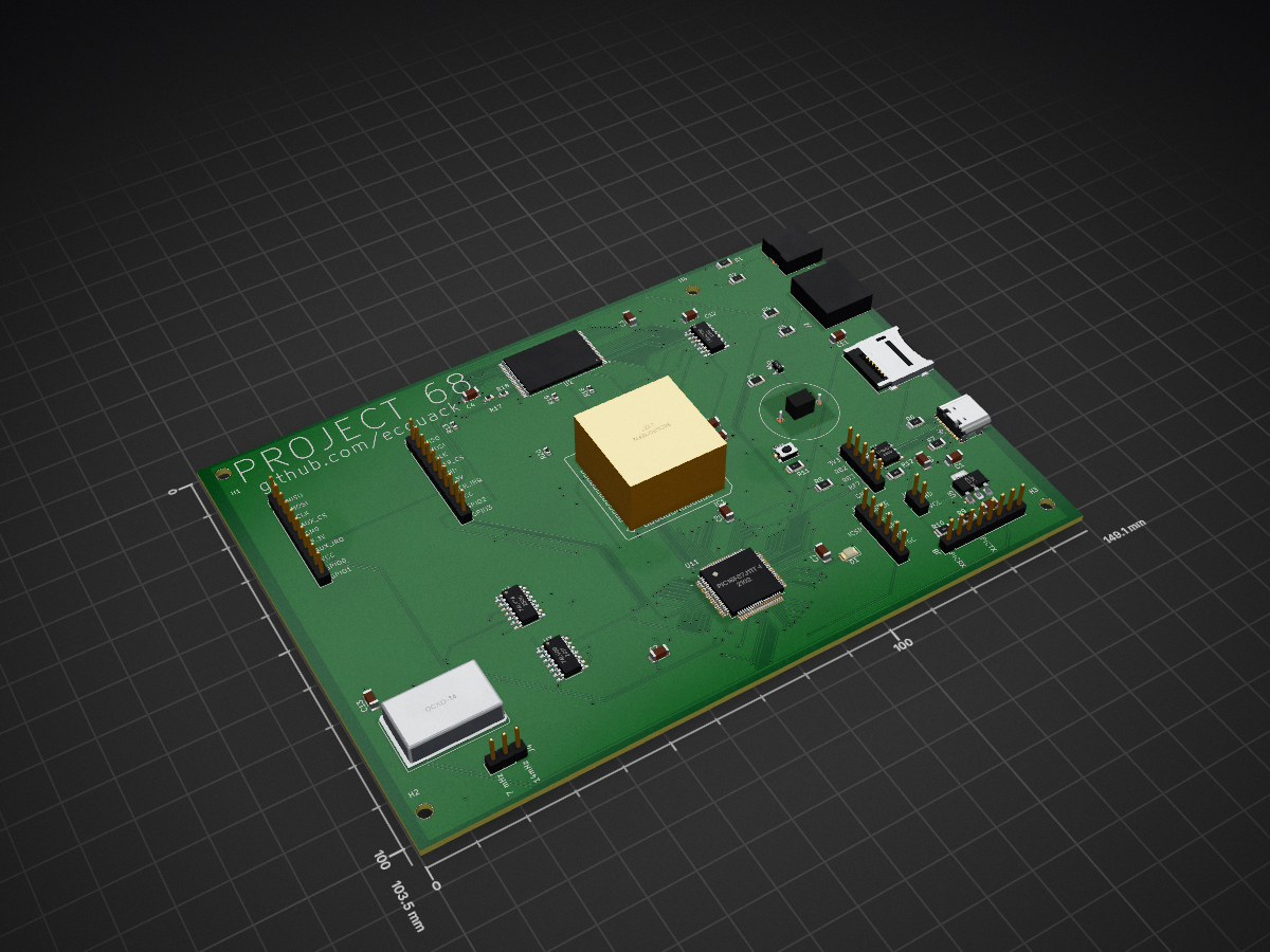
 ecquack/Project68
Project68 is a Motorola MC68xxx 16/32 bit single board computer with an 8 bit PIC18 co-processor.
Project68 is an open-source printed circuit board by ecquack, from the ecquack/Project68 repository on GitHub, published under the MIT licence. It is a 4-layer board of 149.1 × 103.5 mm with 61 parts on 124 nets, routed with 1,633 tracks and 221 vias.
It is built around the CH340N, 74HCT30D and 74LV00D, with the 74LV74D, AMS1117-3.3 and MD-60S among its other parts. Its parts include 20 resistors, 13 capacitors, 11 connectors, 8 ICs and 1 diode. It belongs with the PIC boards of this library.


Project68 is a Motorola MC68xxx 16/32 bit single board computer with an 8 bit PIC18 co-processor.
My goal was to do something interesting with the tube of factory new 68008 CPUs that I've been hoarding for 25 years, so I have designed a useful self contained 68K computer using a minumum number of components and special tools.
The system connects directly to a monitor and keyboard and does not require a host computer.
This project is at an early stage of development, but it is intended to run uCLinux 4.4.
Special thanks to crmaykish, creator of the Mackerel-68K project.
The CPU is the 8 bit external bus version of the 68K, the MC68008FN8. It comes in the larger 52 pin PLCC package which can address up to 4 megabytes of memory. The CPU is socketed on the board so that you can use an automated assembly service such as JLC PCB or PCBWAY for all the soldering if you prefer. This is a 16/32 bit CPU internally with a narrow external bus which allows using byte wide external memories.
The parts I have are rated at 8mHz, but 10mHz parts are also available (MC68000FN10). In order to provide an NTSC video clock, the processor runs at ~7.16mHz. Either speed part can (usually) be successfully overclocked to ~14.318mHz without issue. An overclocking jumper is provided if you feel the need for speed.
The system has four megabytes of memory. It uses a single 32 megabit 4Mx8 55ns SRAM chip. This fills the entire available address space with SRAM. There is no separate FLASH, EPROM, or ROM memory, no address decoding of any kind, no special address hardware at reset, and no traditional memory mapped I/O. Just an unbroken sea of RAM from 0-0x3FFFFF and a simple _DTACK generator.
The SRAM part is a fairly pricey Renesas RMLV3216AGSA-5S2 sourced from Digikey. You can also use the pin compatible Alliance AS6C6416-55TIN from Mouser which is a 64 megabit part, which is actually cheaper, but you will only be utilizing half the memory.
The memory and the PIC18 run at 3.3 volts (there is an LDO regulator on the board). The 5 volt MC68008 has a logic high level of 2.4 volts, which might be safe to use with these parts. I may end up using level shifters, but they eat 20 nanoseconds from the bus cycle. Stay tuned for my experimental results.
The PIC18F87J11 microcontroller comes in an 80 pin TQFP package. This part was chosen because it has enough GPIO pins to emulate the entire MC68008 bus. It has 128K of FLASH memory, and just under 4K of on chip SRAM.
The PIC18 co-processor provides all the main processor’s I/O using soft-DMA. When it is time to transfer data to or from the processor, the co-processor requests the bus from the 68008. When the bus is granted, it uses bit-banging DMA to read and write the SRAM. A few specific addresses in the memory space are designated as I/O command and status registers and are interpreted as such by the co-processor to provide low level BIOS functions for the console, serial port, and SD card.
At power up the co-processor asserts _HALT and _RESET and then copies up to 64K of BIOS into the SRAM from the upper half of FLASH memory that’s built into the PIC18. It then releases the 68K bus and the MC68008 starts.
The co-processor is also responsible for generating the 80x25 video display. This is done with a really tight horizontal sync interrupt handler written in assembly language. It uses an interleaved character FLASH lookup table with an 8x8 pixel font. One EUSART on the PIC18 is used as a video shift register (nice!), which makes it possible to clock pixels out once per instruction cycle.
Roughly half of the PIC18's SRAM (2K) is dedicated to the video display.
The physical video interface consists of two output pins and a two resistor network that is connected to an RCA jack. One pin is the output of the synchronous serial transmitter, and the other is the software generated sync line, used for both horizontal and vertical sync.
The video display is not interlaced and does not include a colorburst. The 8x8 ROM font consists of the standard printable ASCII characters (codes 32-126), plus a number of special characters (codes 0-31 and 127). The upper 128 characters are reverse video of the lower 128 characters, which is used to generate the cursor. There are no fancy effects like blink, underscore, or dim. There are no code page 437 special characters.
Most of the co-processor's time is spent generating video. There is a short horizontal blanking period at the end of each line, and there is a longer vertical blanking interval at the end of each video field during which the processor is free to perform other tasks. All video generation (and PS/2 keyboard processing) takes place inside the interrupt handler.
Note that it should be possible to run a PAL monitor instead of NTSC by simply adjusting the timing #DEFINE statements in the beginning of 80columnvideo.h. I do not have a monitor that accepts PAL video to test this with.
The system uses the PIC18 MSSP (synchronous serial port) in slave mode with an assembly language interrupt handler to interface to the PS/2 keyboard. The interrupt handler runs during horizontal blanking, and always takes the same number of clock cycles to run, no matter which code path is taken, to avoid disturbing the video output.
When characters arrive on the PS/2 keyboard or serial port, the co-processor requests the bus, and stores the received characters into a software FIFO in SRAM.
The SD card socket is connected to the PIC18 over the shared SPI bus. 512 bytes of PIC18 SRAM is reserved to store a single block of data to/from the SD card.
The BIOS provides a few functions to access the console, the serial port, and the SD card. It also loads and starts Linux from the SD card. Additional functions could be added, for example, to copy the entire screen buffer to and from memory, give control over the PWM audio output beyond the fixed "beep", or to support additional SPI devices such as a non-volatile real time clock.
The vertical blanking signal serves as a periodic timer interrupt (60 hertz) to the 68008. This is used by the BIOS for communication and by the Linux kernel for timekeeping and task switching.
A CH340N provides a very basic serial port connection to a USB host system. The USB C connector also provides power to the board. There is also a header with jumpers that allow the TTL serial lines to be disconnected from the USB chip and used directly.
There are two main expansion ports. Each has power, SPI bus, it's own SPI chip select, it's own interrupt line, and two GPIO pins. My intention is to use an SPI DUAL UART on one port and an SPI RTC on the other. Supporting these will require additions to the BIOS. The interrupt line and the chip select can be used as GPIOs if the SPI bus is not used, but MISO, MOSI, and SCLK are shared with the SD card socket and cannot be reassigned.
There is also a third expansion port which brings out the three unused PIC18 GPIO pins, power, and ground. Two of these pins are on port B and can be used as interrupt sources.
For programming the PIC MCU, this 6 pin connector contains PGD, PGC, _MCLR, +5V, and GND.
The current system was designed to see how simply a complete 68K computer system could be made, and it uses a minimum number of parts for a system that has its own video and keyboard interfaces. By adding just a few chips you can dramatically increase the performance of the system.
For higher overall system performance you could use a second smaller PIC18 (such as a PIC18F26K22) dedicated to generating video. Right now there is an I/O bottleneck because I/O operations are only performed during video blanking.
A decoded address that causes an interrupt on the PIC18 would eliminate the need for the PIC18 to poll the MC68008's memory. Again, this would increase performance but it would add chips to the design and eat into the memory address space. Two 74HCT30s and a 74HCT00 would suffice, and would eat only 64 bytes from the memory map.
*note that there is a 45 day free trial of this compiler.
I started out with a tube full of sixteen 68008 parts that I got from a Motorola rep back in the '90s. I'm keeping a few chips for myself and my friends, but I may have a few pre-assembled boards complete with CPUs and SD cards for sale at some point.
Note that the MC68008FN is no longer in production, but at this time (August, 2025) it is not difficult to find them on eBay for around USD$30 with shipping.
The schematic capture and layout of the first version is complete. I'll order the blank boards and stencil from JLCPCB next.
I wrote the PIC18 80 column video code and the PS/2 keyboard handler code back in 2010 and posted them to the CCS C compiler forum. They were tested on a single sided PIC18F26J11 board that I milled on my CNC machine back in the day.
Once the layout is complete I plan to have a pair of assembled boards made for my by JLCPCB.
After that, the next debugging steps are:
Then comes the work of writing the BIOS and building the linux image.
| Qty | Value | Footprint | References |
|---|---|---|---|
| 8 | 0.1uF | Capacitor_SMD:C_1206_3216Metric | C3, C4, C5, C7, C8, C9, C12, C13 |
| 8 | 10K | Resistor_SMD:R_0603_1608Metric | R13, R14, R15, R16, R17, R18, R19, R20 |
| 4 | 10uF | Capacitor_SMD:C_1206_3216Metric | C1, C6, C10, C11 |
| 4 | 1K | Resistor_SMD:R_1206_3216Metric | R3, R9, R10, R12 |
| 4 | 5K1 | Resistor_SMD:R_1206_3216Metric | R4, R5, R6, R7 |
| 4 | MountingHole | MountingHole:MountingHole_3.2mm_M3 | H1, H2, H3, H4 |
| 1 | 10K | Resistor_SMD:R_1206_3216Metric | R11 |
| 1 | 10uF tantalum | Capacitor_SMD:C_1206_3216Metric | C2 |
| 1 | 220 | Resistor_SMD:R_1206_3216Metric | R8 |
| 1 | 330 | Resistor_SMD:R_1206_3216Metric | R1 |
| 1 | 680 | Resistor_SMD:R_1206_3216Metric | R2 |
| 1 | 74HCT30 | Package_SO:SOIC-14_3.9x8.7mm_P1.27mm | U1 |
| 1 | 74LV00 | Package_SO:SOIC-14_3.9x8.7mm_P1.27mm | U3 |
| 1 | 74LV74 | Package_SO:SOIC-14_3.9x8.7mm_P1.27mm | U4 |
| 1 | AMS1117-3.3 | Package_TO_SOT_SMD:SOT-223-3_TabPin2 | U5 |
| 1 | Buzzer | equack:MURATA | BZ1 |
| 1 | CH340N | Package_SO:SOP-8_3.9x4.9mm_P1.27mm | U6 |
| 1 | Conn_01x08_Pin | Connector_PinHeader_2.54mm:PinHeader_1x08_P2.54mm_Vertical | J8 |
| 1 | Expansion 3 | Connector_PinHeader_2.54mm:PinHeader_1x05_P2.54mm_Vertical | J7 |
| 1 | ICSP | Connector_PinHeader_2.54mm:PinHeader_1x06_P2.54mm_Vertical | J9 |
| 1 | LED | LED_SMD:LED_1206_3216Metric | D1 |
| 1 | MC68008FN | MC68008FN:PLCC52-S | IC1 |
| 1 | MD-60S | MD-60S:CUI_MD-60S | J2 |
| 1 | Micro_SD_Card | Connector_Card:microSD_HC_Molex_47219-2001 | J3 |
| 1 | NPN | Package_TO_SOT_SMD:SOT-23-3 | Q1 |
| 1 | OCXO-14 | Oscillator:Oscillator_DIP-14 | Y1 |
| 1 | Overclock jumper | Connector_PinHeader_2.54mm:PinHeader_1x03_P2.54mm_Vertical | J4 |
| 1 | PIC18F87J11T-I_PT | PIC18F87J11T-I_PT:QFP50P1400X1400X120-80N | U11 |
| 1 | POWER INPUT | Connector_PinHeader_2.54mm:PinHeader_1x02_P2.54mm_Vertical | J6 |
| 1 | RCJ-044 | RCJ-044:CUI_RCJ-044 | J1 |
| 1 | RTC_OPTION | Connector_PinHeader_2.54mm:PinHeader_1x10_P2.54mm_Vertical | J10 |
| 1 | SERIAL_OPTION | Connector_PinHeader_2.54mm:PinHeader_1x10_P2.54mm_Vertical | J11 |
| 1 | SW_SPST | Button_Switch_SMD:SW_Push_1P1T_NO_CK_KMR2 | SW1 |
| 1 | USB_C_Receptacle_USB2.0_14P | Connector_USB:USB_C_Receptacle_GCT_USB4105-xx-A_16P_TopMnt_Horizontal | J5 |
| 1 | ~ | Package_SO:TSOP-I-48_18.4x12mm_P0.5mm | U2 |
It measures 149.1 × 103.5 mm and has 4 copper layers, 1.6 mm thick.
61 parts, built around the CH340N, 74HCT30D, 74LV00D and 74LV74D. The full list of its parts is on this page, with links to each part's symbol and footprint where PCBKit's library has them.
From the ecquack/Project68 repository on GitHub, at the commit this page was made from: the board is KiCAD/Project68.kicad_pcb and its schematic DAUGHTER/DAUGHTER.kicad_sch. PCBKit opens the board in the browser, with nothing to install.
Its repository publishes it under the MIT licence: you may reuse it on that licence's terms (keep the author's notice, and for a copyleft licence share your changes alike).

Heer-Boaz/BMSX
This separate project extends the R127 memory candidate by moving the INPUT interface from U7 to U2. The existing cartridge, keyboard and pad connector pinouts remain unchanged. Snapshot selection remains on U2.102.

gildobjanschi/ECP5_BGA381_FT2232HQ_FIFO_EXT
Extension board for the ECP5_BGA381_FT2232HQ_FIFO board


punkfab/pcb-corpus
235 real KiCad boards from open-source hardware repositories, prepared as a placement and routing benchmark

