
2 layers290.1 × 130 mm
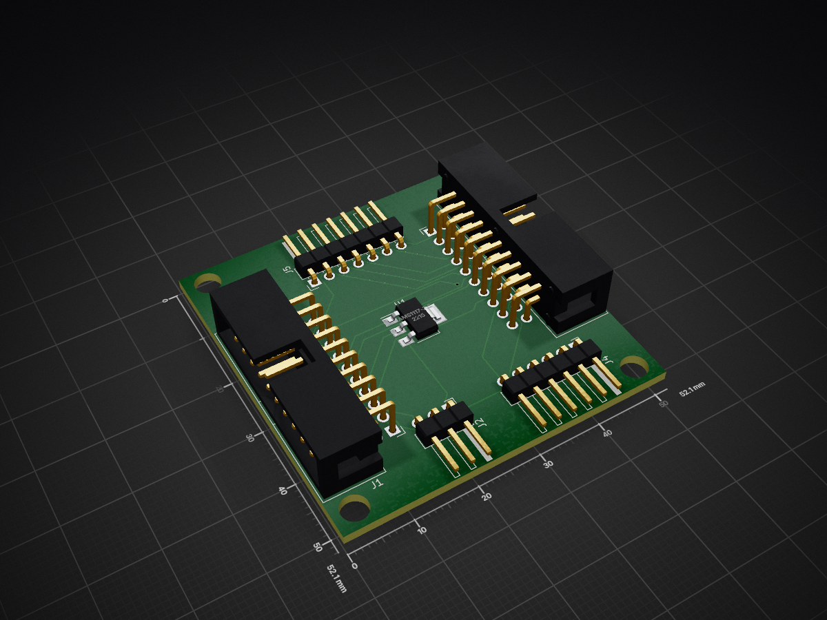
 ebaskale/JLinkMultiPortPCB1
JLinkMultiPortPCB is an open-source printed circuit board by ebaskale, from the ebaskale/JLinkMultiPortPCB repository on GitHub, published under the MIT licence. It is a 2-layer board of 52.1 × 52.1 mm with 6 parts on 24 nets, routed with 212 tracks and 1 via.
It is built around the AMS1117-3.3. Its parts include 5 connectors and 1 IC.
JLink Multi Port PCB is home made, DIY project for JLink. It's an adapter for JLink's 20 pins JTAG interface. It can supply 3V3 and 5V power on various debug interfaces such as SWO, ICSP and JTAG. It has power select jumpers for VSupply and also it's can be used disable supply voltage.
| Qty | Value | Footprint | References |
|---|---|---|---|
| 2 | Conn_02x10_Odd_Even | Connector_IDC:IDC-Header_2x10_P2.54mm_Horizontal | J1, J3 |
| 1 | AMS1117-3.3 | Package_TO_SOT_SMD:SOT-223-3_TabPin2 | U1 |
| 1 | Conn_01x03 | Connector_PinHeader_2.54mm:PinHeader_1x03_P2.54mm_Horizontal | J2 |
| 1 | Conn_01x06 | Connector_PinHeader_2.54mm:PinHeader_1x06_P2.54mm_Horizontal | J4 |
| 1 | Conn_01x07 | Connector_PinHeader_2.54mm:PinHeader_1x07_P2.54mm_Horizontal | J5 |
It measures 52.1 × 52.1 mm and has 2 copper layers, 1.6 mm thick.
6 parts, built around the AMS1117-3.3. The full list of its parts is on this page, with links to each part's symbol and footprint where PCBKit's library has them.
From the ebaskale/JLinkMultiPortPCB repository on GitHub, at the commit this page was made from: the board is JLinkMultiPortPCB.kicad_pcb and its schematic JLinkMultiPortPCB.kicad_sch. PCBKit opens the board in the browser, with nothing to install.
Its repository publishes it under the MIT licence: you may reuse it on that licence's terms (keep the author's notice, and for a copyleft licence share your changes alike).

pascallanger/DIY-Multiprotocol-TX-Module
Multiprotocol TX Module (or MULTI-Module) is a 2.4GHz transmitter module which controls many different receivers and models.

fossasia/pslab-hardware
PSLab Hardware Design and Schematics https://pslab.io


MaltWhiskey/Mega-Cube
16x16x16 PL9823 Cube with Teensy 4.0 and FlexIO driver


shamansystems/Cheap-FOCer-2
Low-Cost Motor Controller based on the VESC 6