2 layers28.5 × 12.3 mm

 dvallemo/CANBUS-Sniffer-PCB
Built a four-layer STM32-based CAN bus sniffer PCB to detect and translate CAN codes from a vehicle
CAN BUS sniffer is an open-source printed circuit board by dvallemo, from the dvallemo/CANBUS-Sniffer-PCB repository on GitHub. It is a 4-layer board of 63 × 55 mm with 46 parts on 56 nets, routed with 348 tracks and 69 vias.
It is built around the CH340E, SN65HVD230D and CH213K, with the USBLC6-2SC6 among its other parts. Its parts include 17 capacitors, 10 resistors, 6 ICs, 4 connectors and 2 diodes. It belongs with the interfaces and adapters boards and the STM32 boards of this library.


A compact USB-to-CAN Bus interface designed around an STM32F0 microcontroller and a CAN transceiver. This project was built to practice professional PCB design techniques from schematic capture through PCB layout while following industry design practices.
Version: V1.0.0
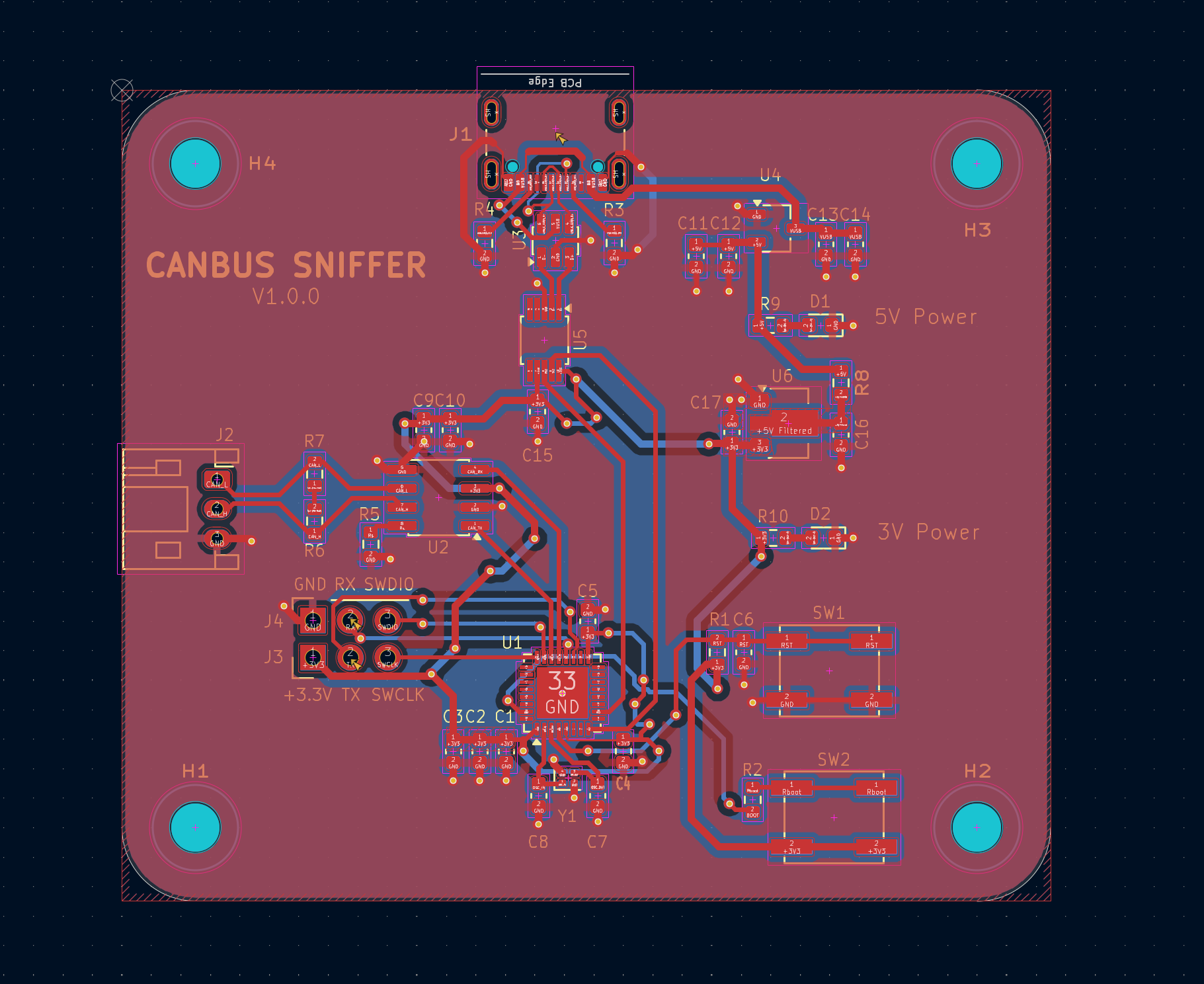
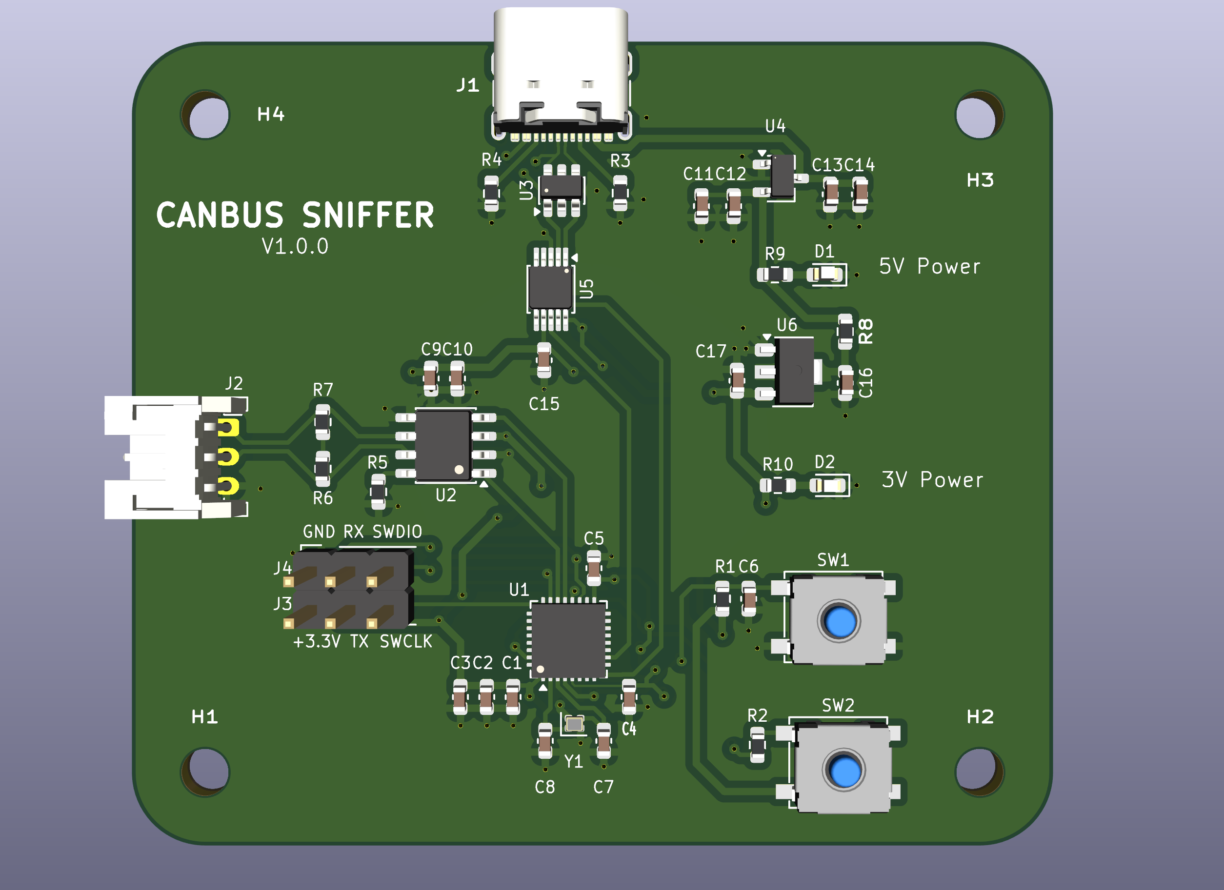
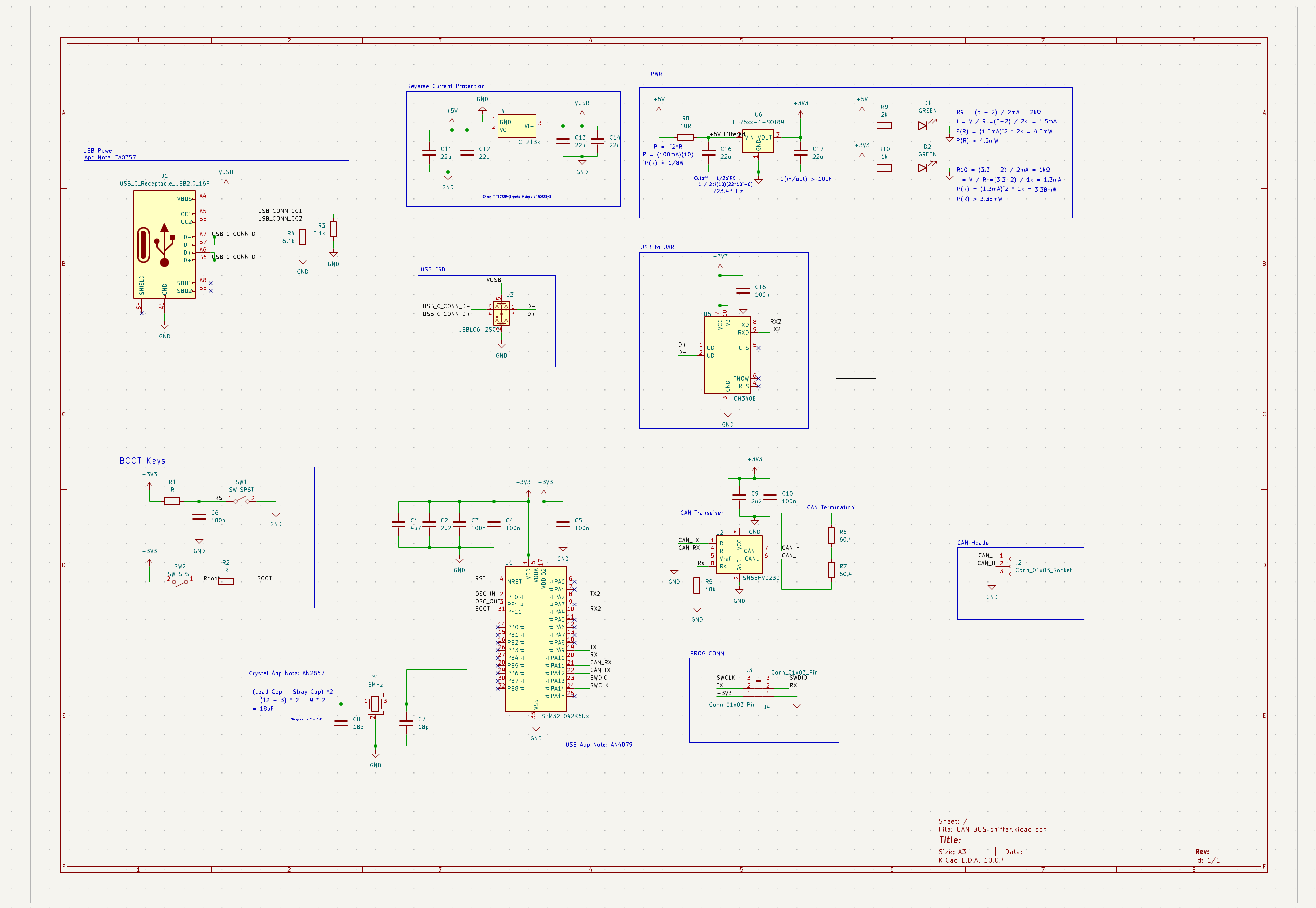
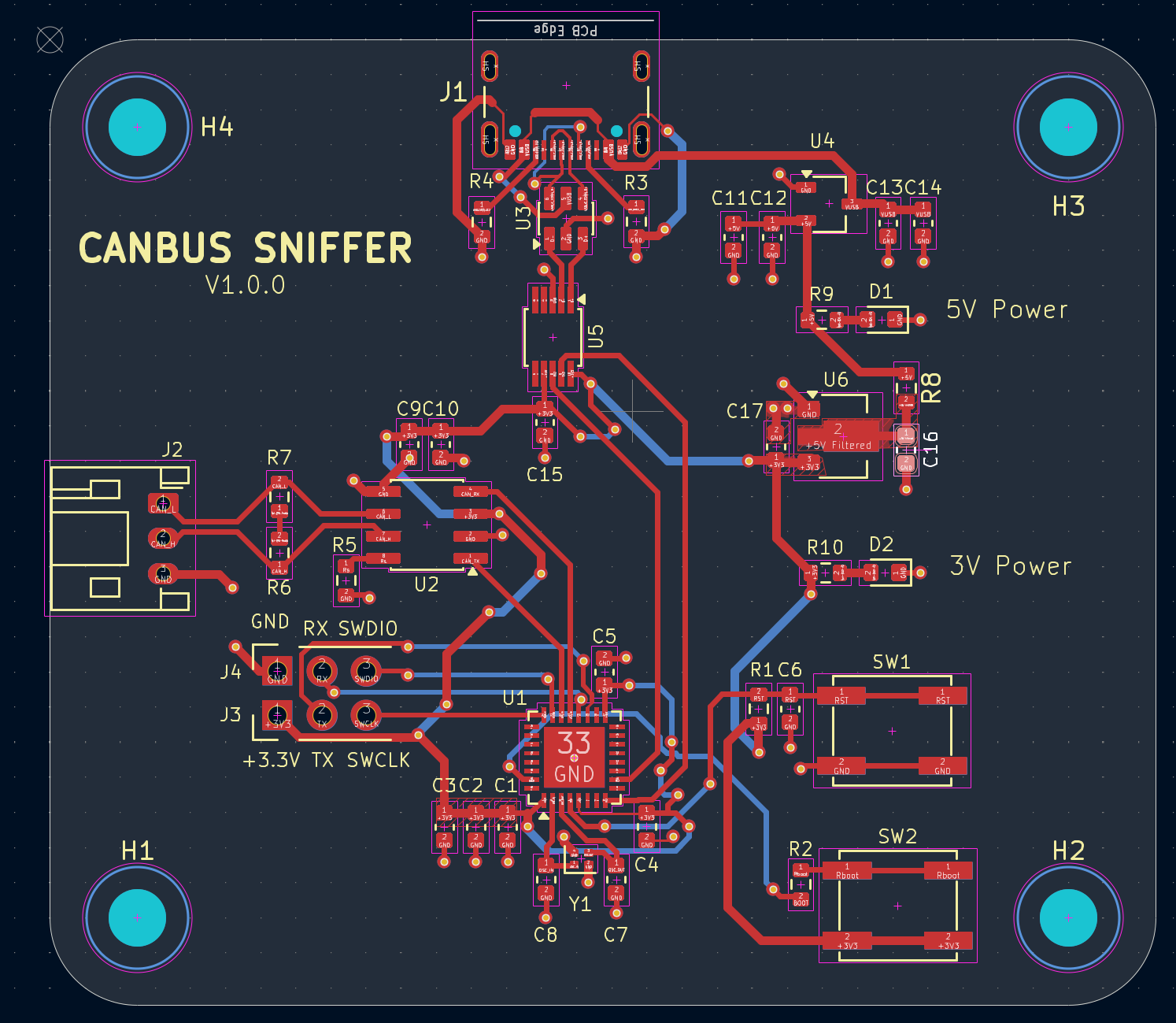
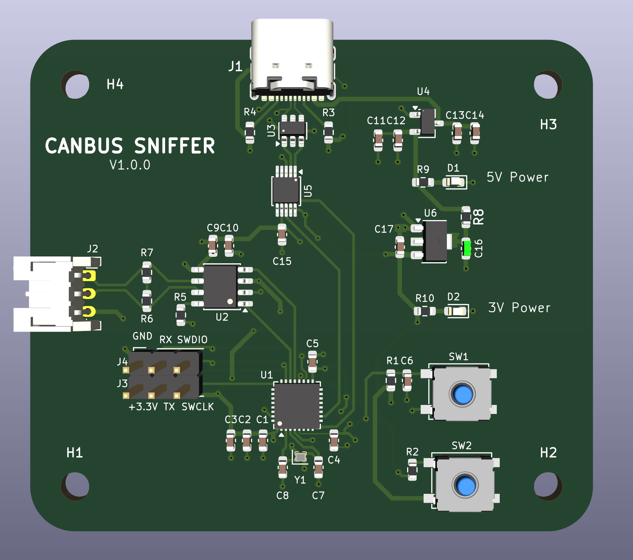
The goal of this project was to design a complete CAN Bus Sniffer PCB using KiCad while applying professional hardware engineering methodologies.
The board receives power over USB Type-C, regulates the voltage to 3.3V, communicates over a CAN transceiver, and provides an SWD interface for programming and debugging.
Rather than only creating a working PCB, this project focused heavily on layout quality, manufacturability, and signal integrity.
Topics practiced include:
| Item | Specification |
|---|---|
| Microcontroller | STM32F0 Series |
| CAN Transceiver | SN65HVD230 Compatible |
| USB | USB Type-C (USB 2.0 Full Speed) |
| Input Voltage | 5V USB |
| Output Voltage | 3.3V |
| PCB Layers | 4 |
| PCB Thickness | 1.6 mm |
| USB Routing | Controlled Impedance Differential Pair |
Using two dedicated internal ground planes provides:
USB Type-C was selected for modern compatibility and ease of use.
USB CC pull-down resistors were implemented to correctly identify the board as a USB device.
The USB D+ and D− lines were routed as a differential pair using KiCad's differential pair router.
Special attention was given to:
Although USB Full-Speed is more forgiving than USB High-Speed, the layout follows professional differential routing practices.
Design considerations included:
Power flow:
USB Type-C
    ↓
Protection Circuit
    ↓
Filtering
    ↓
3.3V LDO
    ↓
STM32 + CAN Transceiver
Wide power traces were used where appropriate to reduce voltage drop and improve current handling.
Each power pin is locally decoupled with ceramic capacitors placed as close as possible to the corresponding IC supply pins.
This reduces:
The board utilizes:
This creates low-impedance return paths and improves signal integrity throughout the design.
The exposed thermal pad underneath the STM32 is connected directly into the internal ground planes through a thermal via.
The CAN transceiver converts the MCU CAN peripheral into differential CANH and CANL signals suitable for automotive communication.
The layout emphasizes:
The crystal and its load capacitors were placed immediately adjacent to the MCU oscillator pins.
This minimizes:
Components were grouped by function:
Keeping functional blocks together improves routing quality and simplifies debugging.
The layout follows several common PCB design guidelines:
This project provided hands-on experience with:
CANBUS-Sniffer-PCB/
│
├── README.md
├── LICENSE
│
├── Hardware/
│   ├── CAN_BUS_sniffer.kicad_pro
│   ├── CAN_BUS_sniffer.kicad_sch
│   ├── CAN_BUS_sniffer.kicad_pcb
│   └── ...
│
├── images/
│   ├── schematic.png
│   ├── pcb_layout.png
│   ├── pcb_layout_w_gndpours.png
│   ├── pcb_3d.png
│   └── pcb_3d_w_gndpours.png
│
├── Manufacturing/
│
└── Firmware/This project is released under the MIT License.
Designed by David Valle
Electrical Engineer | PCB Design | Embedded Systems
| Qty | Value | Footprint | References |
|---|---|---|---|
| 6 | 100n | Capacitor_SMD:C_0603_1608Metric | C3, C4, C5, C6, C10, C15 |
| 6 | 22u | Capacitor_SMD:C_0603_1608Metric | C11, C12, C13, C14, C16, C17 |
| 4 | MountingHole | MountingHole:MountingHole_3.2mm_M3_ISO7380 | H1, H2, H3, H4 |
| 2 | 18p | Capacitor_SMD:C_0603_1608Metric | C7, C8 |
| 2 | 2u2 | Capacitor_SMD:C_0603_1608Metric | C2, C9 |
| 2 | 5.1k | Resistor_SMD:R_0603_1608Metric | R3, R4 |
| 2 | 60.4 | Resistor_SMD:R_0603_1608Metric | R6, R7 |
| 2 | Conn_01x03_Pin | Connector_PinHeader_2.54mm:PinHeader_1x03_P2.54mm_Vertical | J3, J4 |
| 2 | GREEN | LED_SMD:LED_0603_1608Metric | D1, D2 |
| 2 | R | Resistor_SMD:R_0603_1608Metric | R1, R2 |
| 2 | SW_SPST | Button_Switch_SMD:SW_SPST_EVQP0 | SW1, SW2 |
| 1 | 10R | Resistor_SMD:R_0603_1608Metric | R8 |
| 1 | 10k | Resistor_SMD:R_0603_1608Metric | R5 |
| 1 | 1k | Resistor_SMD:R_0603_1608Metric | R10 |
| 1 | 2k | Resistor_SMD:R_0603_1608Metric | R9 |
| 1 | 4u7 | Capacitor_SMD:C_0603_1608Metric | C1 |
| 1 | 8MHz | Crystal:Crystal_SMD_1210-4Pin_1.2x1.0mm | Y1 |
| 1 | CH213k | Package_TO_SOT_SMD:TSOT-23 | U4 |
| 1 | CH340E | Package_SO:MSOP-10_3x3mm_P0.5mm | U5 |
| 1 | Conn_01x03_Socket | Connector_JST:JST_PH_S3B-PH-K_1x03_P2.00mm_Horizontal | J2 |
| 1 | HT75xx-1-SOT89 | Package_TO_SOT_SMD:SOT-89-3 | U6 |
| 1 | SN65HVD230 | Package_SO:SOIC-8_3.9x4.9mm_P1.27mm | U2 |
| 1 | STM32F042K6Ux | Package_DFN_QFN:QFN-32-1EP_5x5mm_P0.5mm_EP3.45x3.45mm | U1 |
| 1 | USBLC6-2SC6 | Package_TO_SOT_SMD:SOT-23-6 | U3 |
| 1 | USB_C_Receptacle_USB2.0_16P | Connector_USB:USB_C_Receptacle_GCT_USB4105-xx-A_16P_TopMnt_Horizontal | J1 |


xlazam01/AstroUniBoard
STM32G0B1-based telescope focuser/rotator controller — OnStepX firmware port + KiCad PCB


It measures 63 × 55 mm and has 4 copper layers, 1.59 mm thick.
46 parts, built around the CH340E, SN65HVD230D, CH213K and USBLC6-2SC6. The full list of its parts is on this page, with links to each part's symbol and footprint where PCBKit's library has them.
From the dvallemo/CANBUS-Sniffer-PCB repository on GitHub, at the commit this page was made from: the board is CAN_BUS_sniffer.kicad_pcb and its schematic CAN_BUS_sniffer.kicad_sch. PCBKit opens the board in the browser, with nothing to install.
Its repository states no licence, so its author keeps all rights: ask dvallemo before reusing the design.