2 layers98 × 27 mm

 dvallemo/Shine-On
A simple 2-layer LED indicator board designed to plug into a Raspberry Pi 4 GPIO header. Built as a hands-on exercise in schematic capture, PCB layout, component selection, DFM, and hand soldering.
Shine is an open-source printed circuit board by dvallemo, from the dvallemo/Shine-On repository on GitHub. It is a 2-layer board of 25.4 × 25.4 mm with 5 parts on 12 nets, routed with 24 tracks and 0 vias.
Its parts include 2 resistors, 2 diodes and 1 connector.
A simple 2-layer LED indicator board designed to plug into a Raspberry Pi 4 GPIO header. Built as a hands-on exercise in schematic capture, PCB layout, component selection, DFM, and hand soldering.
Designed in: KiCad
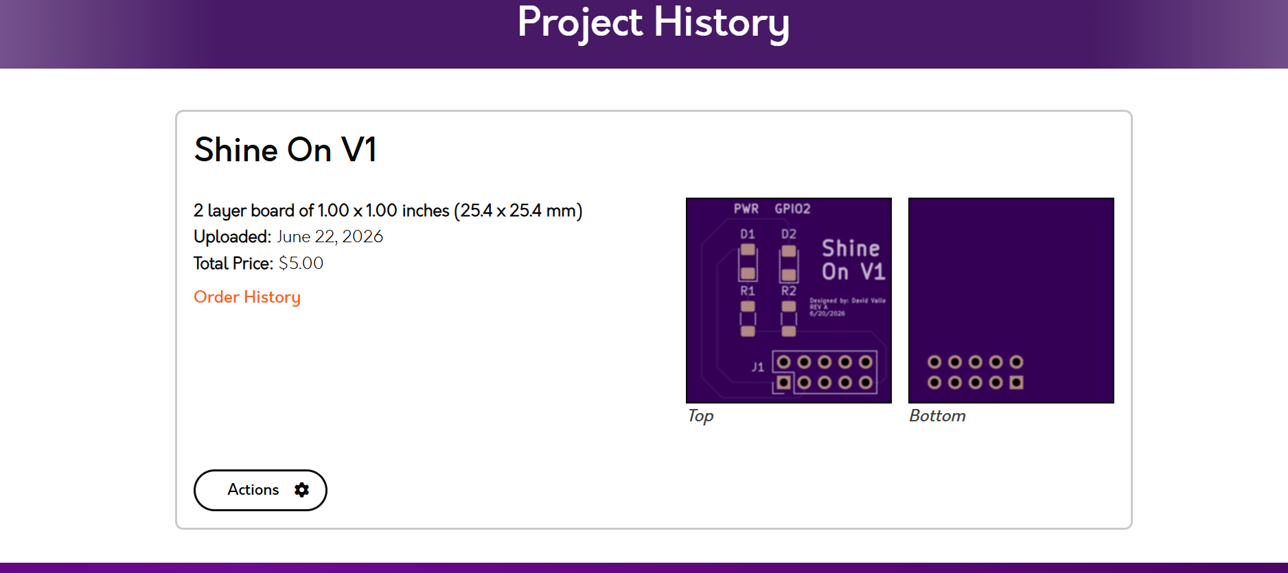
Fabricated by: OSHPark ($5.00 for 3 boards)
Components sourced from: DigiKey
Assembly: Hand soldered by designer
Board size: 25.4 x 25.4 mm (1.00 x 1.00 in), 2-layer
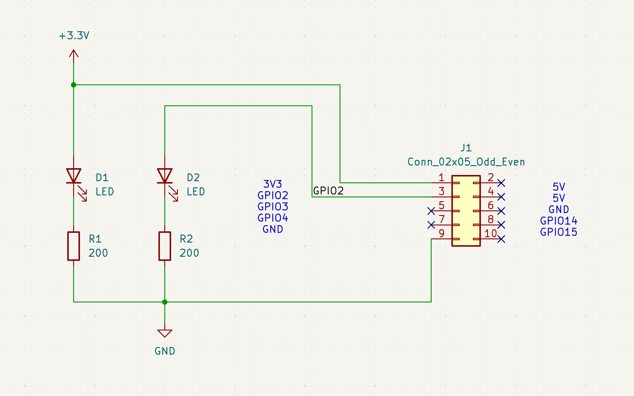
Both LEDs are driven in a simple series configuration:
Current limiting resistors R1 and R2 are 200 ohm, 1/4 W rated, 1206 package. At 3.3V with a typical LED forward voltage of ~2.0V:
I = (3.3V - 2.0V) / 200 ohm = ~6.5 mA
Well within GPIO drive capability (~16 mA max) and LED ratings. Power dissipation per resistor ~8.5 mW, well under the 250 mW rating.
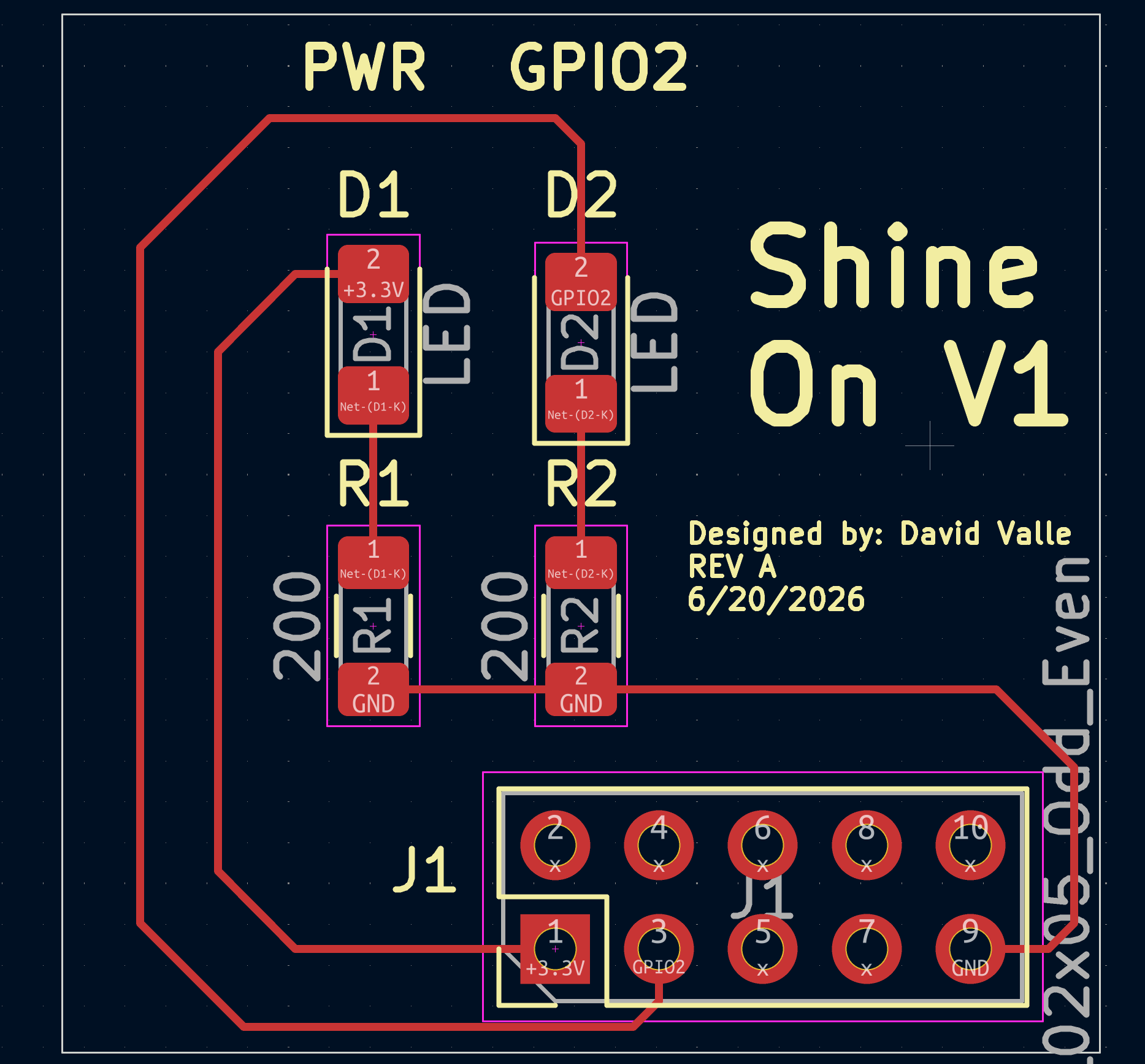
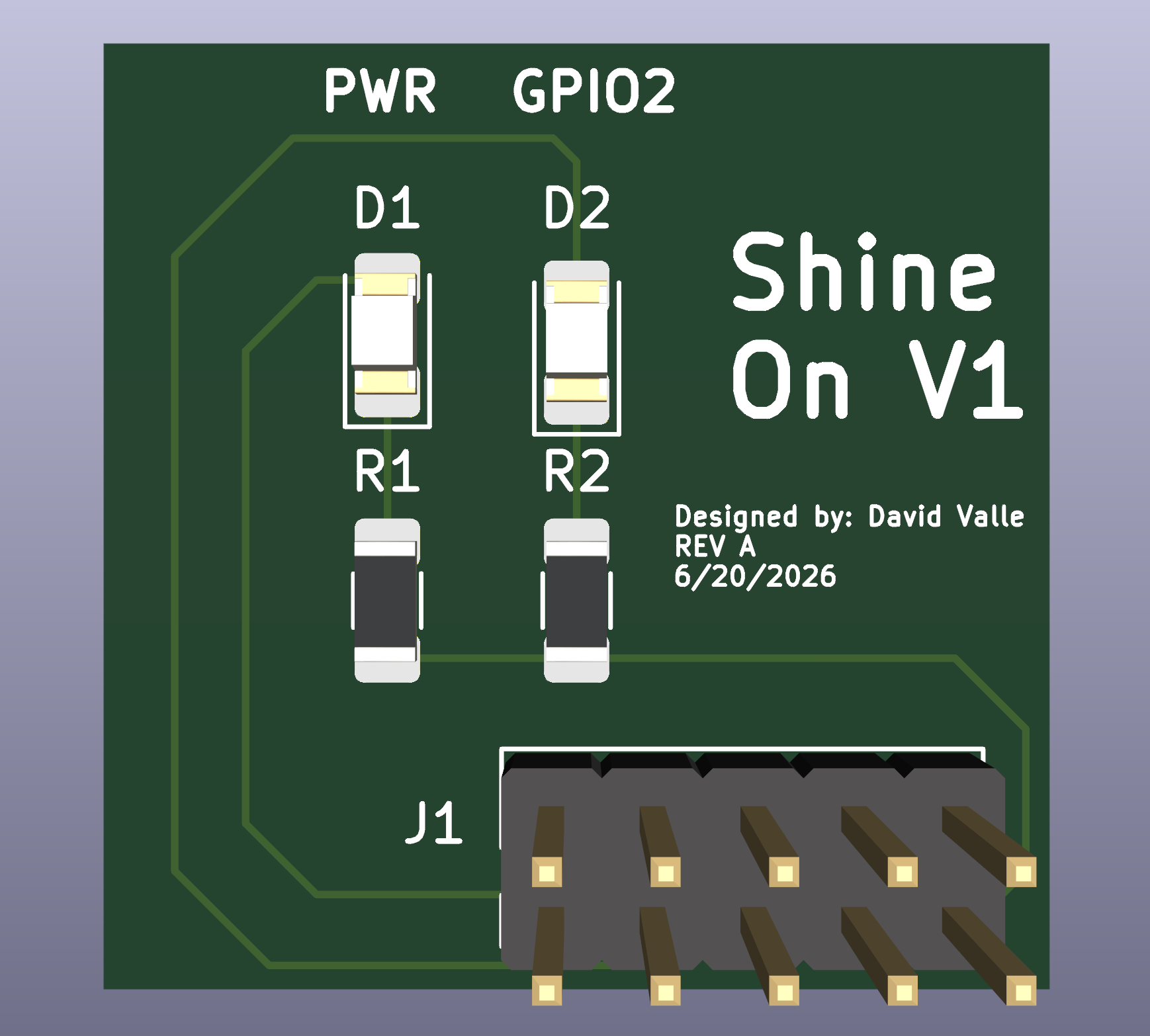
The 10-pin dual-row header (J1) connects directly to the Raspberry Pi 4 GPIO header, exposing +3.3V, GPIO2, and GND.
| Ref | Description | Part Number | Qty | Unit Price |
|---|---|---|---|---|
| R1, R2 | RES 200 ohm 5% 1/4W 1206 | 311-200ERCT-ND (RC1206JR-07200RL) | 50 | $0.027 |
| D1, D2 | Blue LED Surface Mount 1206 | 1568-17734-ND (17734) | 10 | $0.310 |
| J1 | Female Header 2x5 2.54mm Vertical THT | 4324-FHMD-DA010G1NBON-B-ND | 10 | $0.498 |
Components ordered from DigiKey (Order #99956045), shipped 6/22/2026.
Footprints used:
LED_SMD:LED_1206_3216Metric_Pad1.42Resistor_SMD:R_1206_3216Metric_Pad1.42Connector_PinHeader_2.54mm:PinHeader_2x05_P2.54mm_VerticalFabricator: OSHPark
Stack-up: 2-layer, 1 oz copper, purple solder mask, ENIG finish
Board cost: $5.00 (includes 3 copies)
Uploaded: June 22, 2026
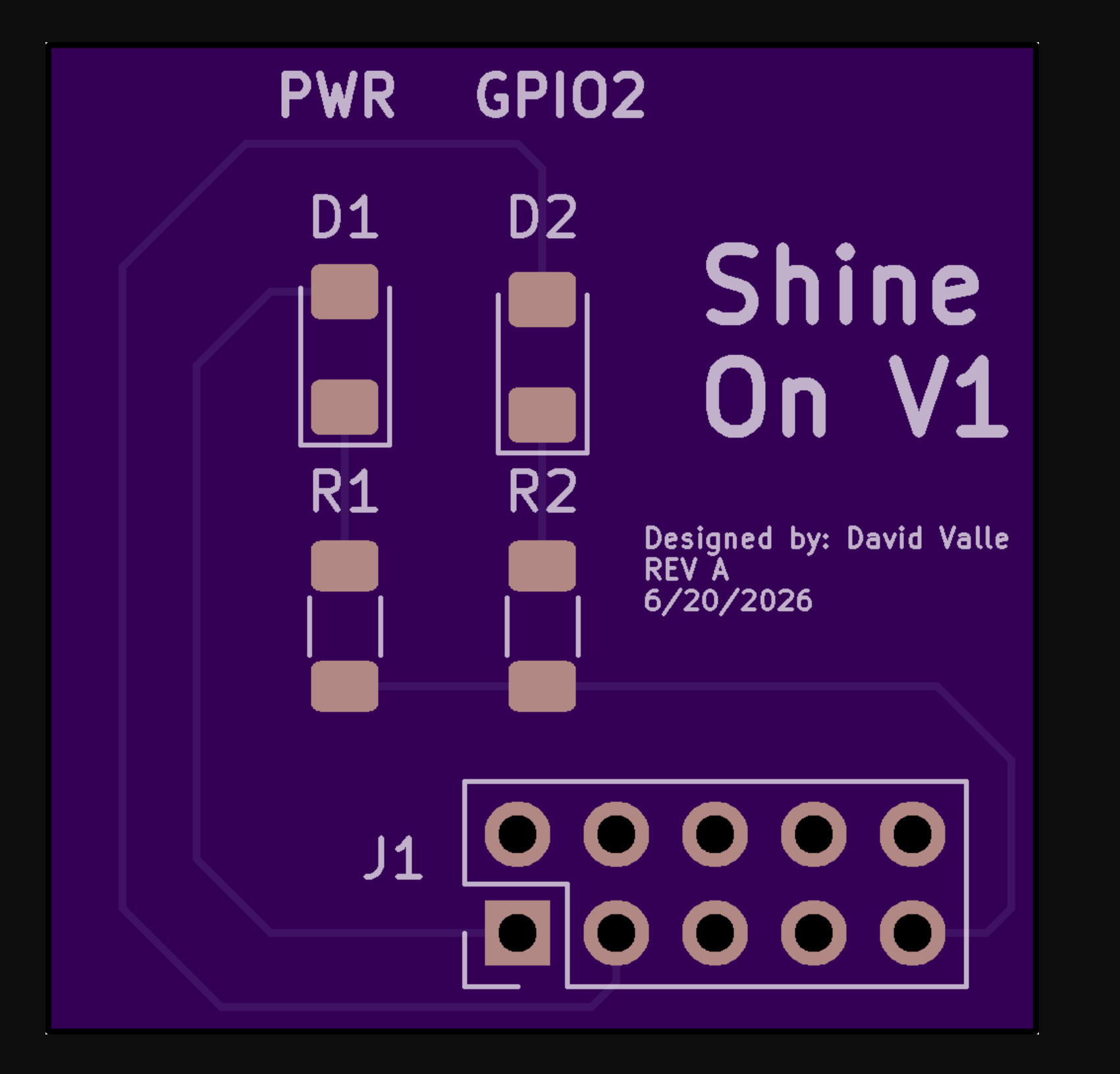
OSHPark renders:
shine-on-v1/
├── kicad/
├── gerbers/
├── images/
├── bom/
└── README.mdDavid Valle
Electrical Engineering, Stevens Institute of Technology
REV A -- June 20, 2026
| Qty | Value | Footprint | References |
|---|---|---|---|
| 2 | 200 | Resistor_SMD:R_1206_3216Metric_Pad1.30x1.75mm_HandSolder | R1, R2 |
| 2 | LED | LED_SMD:LED_1206_3216Metric_Pad1.42x1.75mm_HandSolder | D1, D2 |
| 1 | Conn_02x05_Odd_Even | Connector_PinHeader_2.54mm:PinHeader_2x05_P2.54mm_Vertical | J1 |
It measures 25.4 × 25.4 mm and has 2 copper layers, 1.6 mm thick.
5 parts. The full list of its parts is on this page, with links to each part's symbol and footprint where PCBKit's library has them.
From the dvallemo/Shine-On repository on GitHub, at the commit this page was made from: the board is Shine.kicad_pcb and its schematic Shine.kicad_sch. PCBKit opens the board in the browser, with nothing to install.
Its repository states no licence, so its author keeps all rights: ask dvallemo before reusing the design.

joypad-ai/joypad-os
Universal controller firmware for building adapters, dongles, and custom controllers.

OLIMEX/OLINUXINO
OLINUXINO is Open Source / Open Hardware, low cost from EUR 24 Linux Industrial grade Single Board Computer capable to operate -25+85C

jamro/tiny-engineer
A small desktop robot that brings an AI coding assistant to life, physically acting out when it reads files, thinks, writes code, and finishes work.

hackclub/OnBoard
💡 Join 1,000 teenagers and make your first PCB with a $100 grant!


Luos-io/luos_engine
Open-source and real-time orchestrator for cyber-physical-systems, to easily design, test and deploy embedded applications and digital twins.