2 layers182.2 × 116.6 mm

 dlip/tenshi40
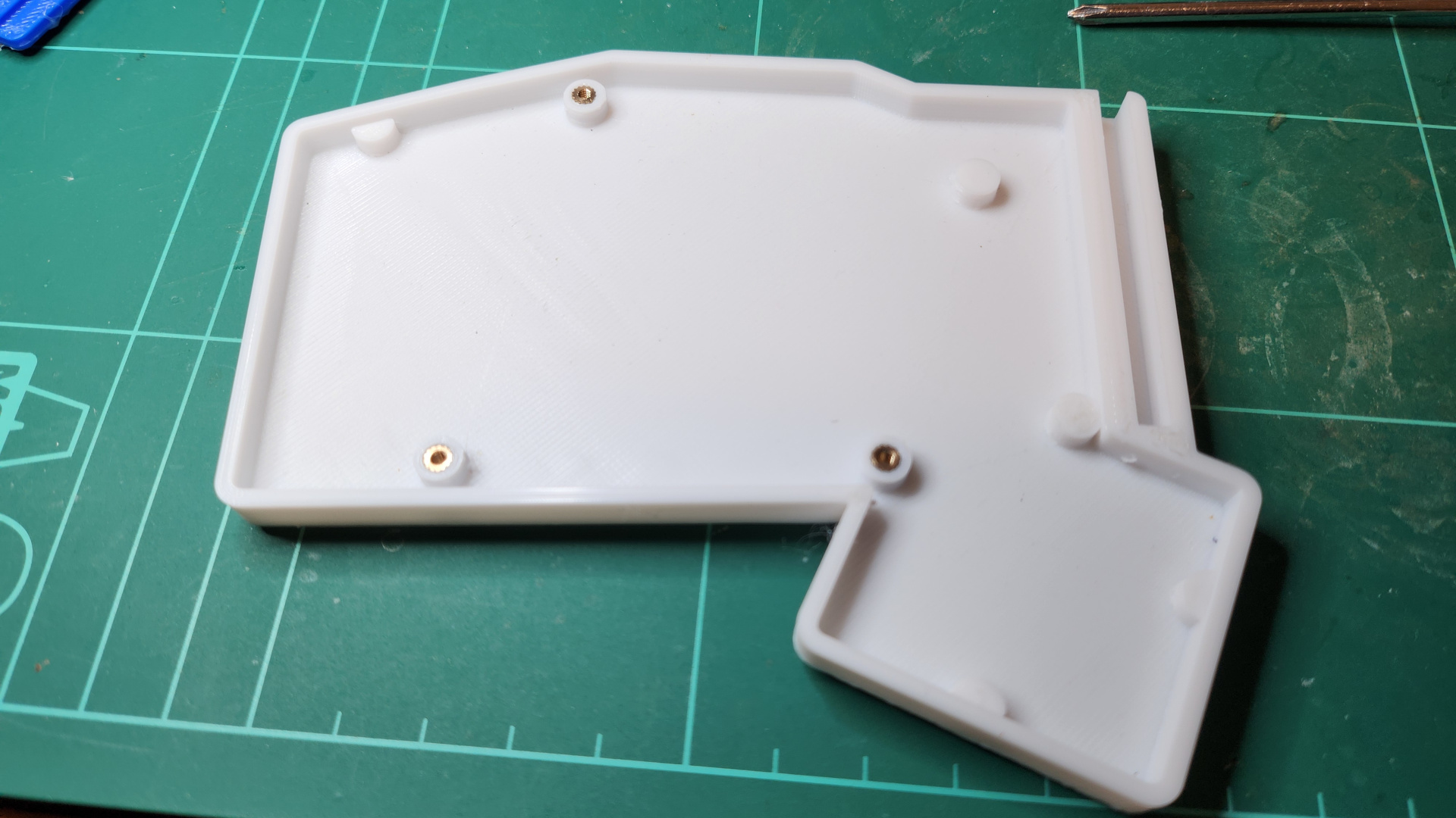
The .stls are in the printables folder and there is also the OnShape Project in case you want to make modifications.
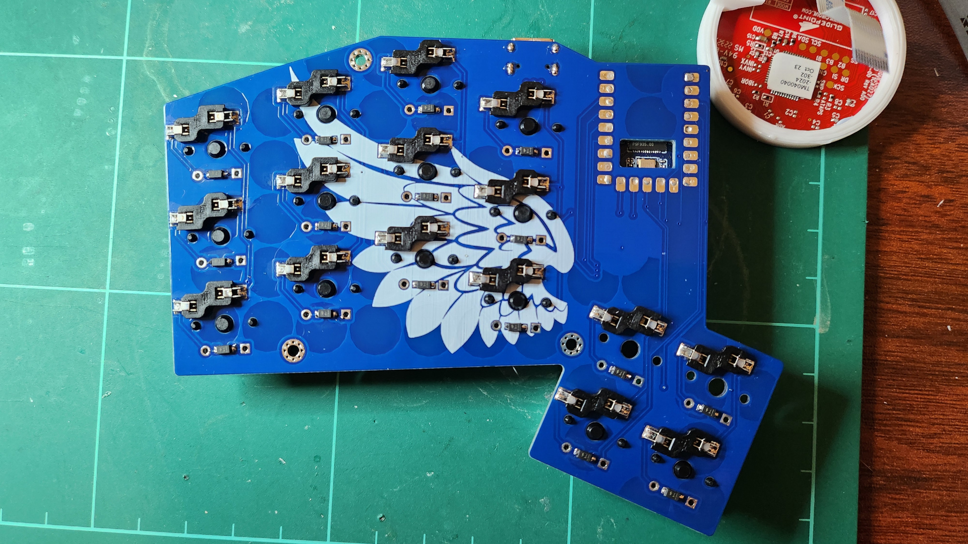
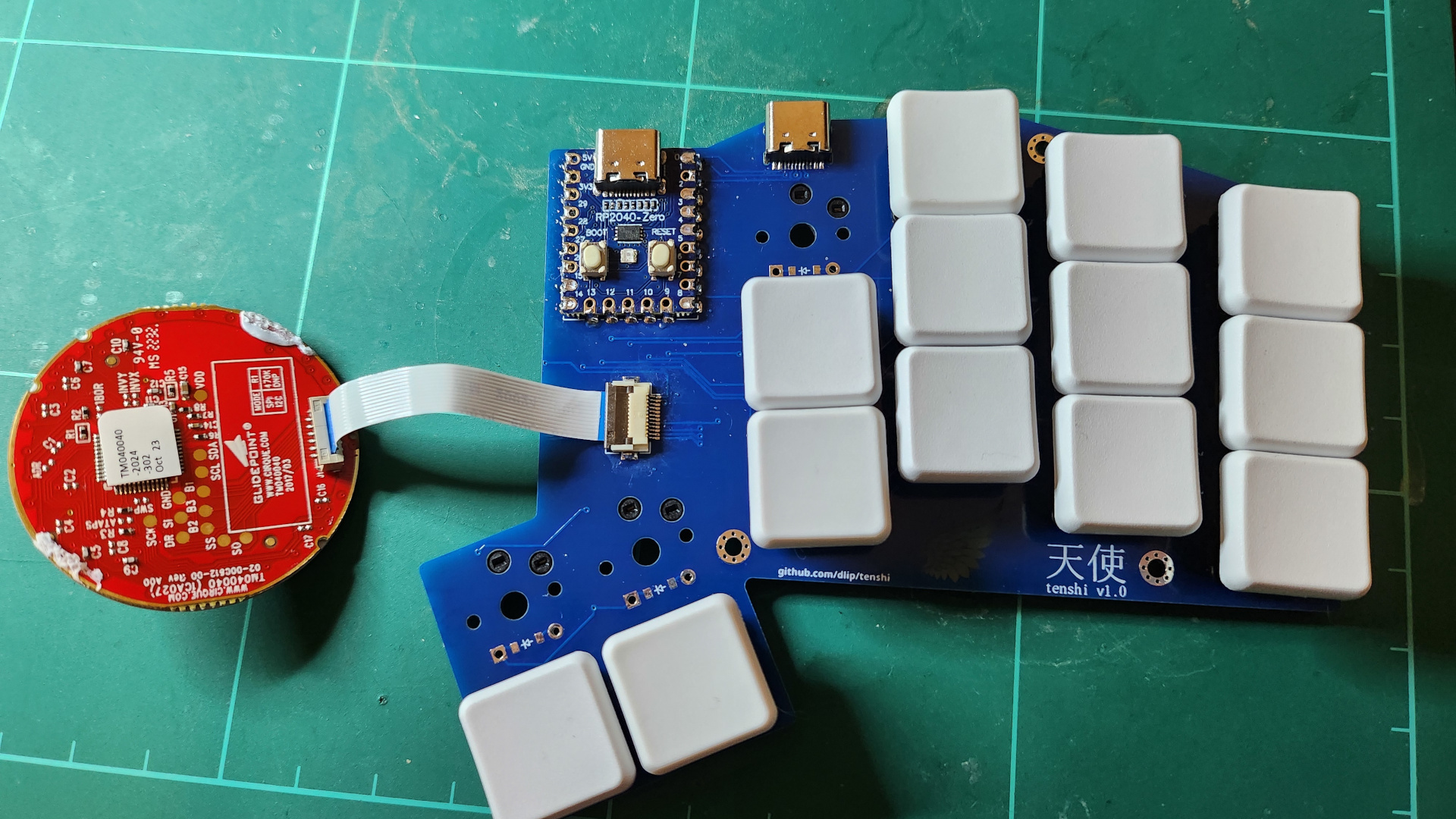
Tenshi is an open-source printed circuit board by dlip, from the dlip/tenshi repository on GitHub, published under the GPL-3.0 licence. It is a 2-layer board of 262.6 × 94.4 mm with 84 parts on 78 nets, routed with 868 tracks and 43 vias.
Its parts include 32 diodes and 32 switches.
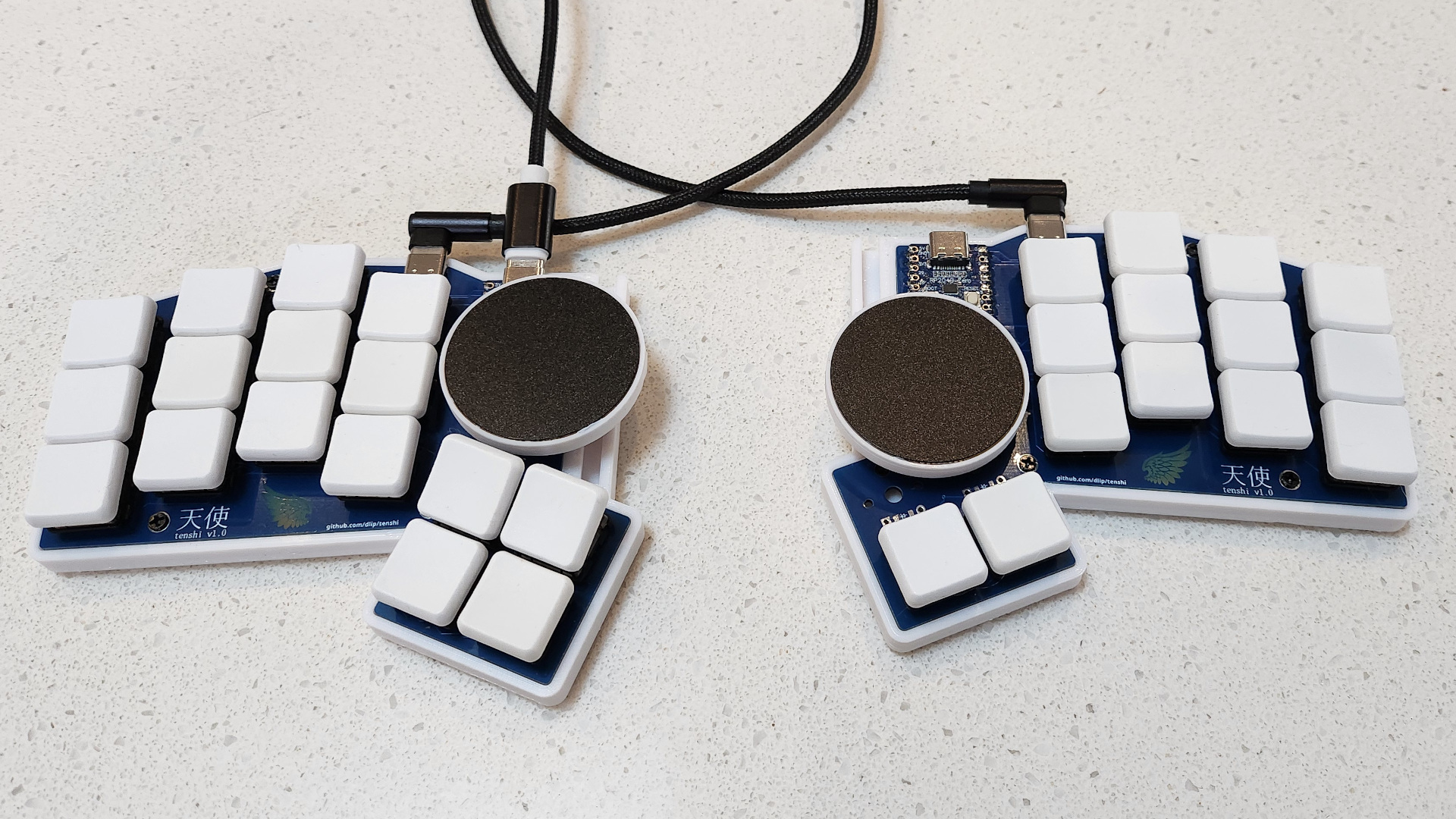
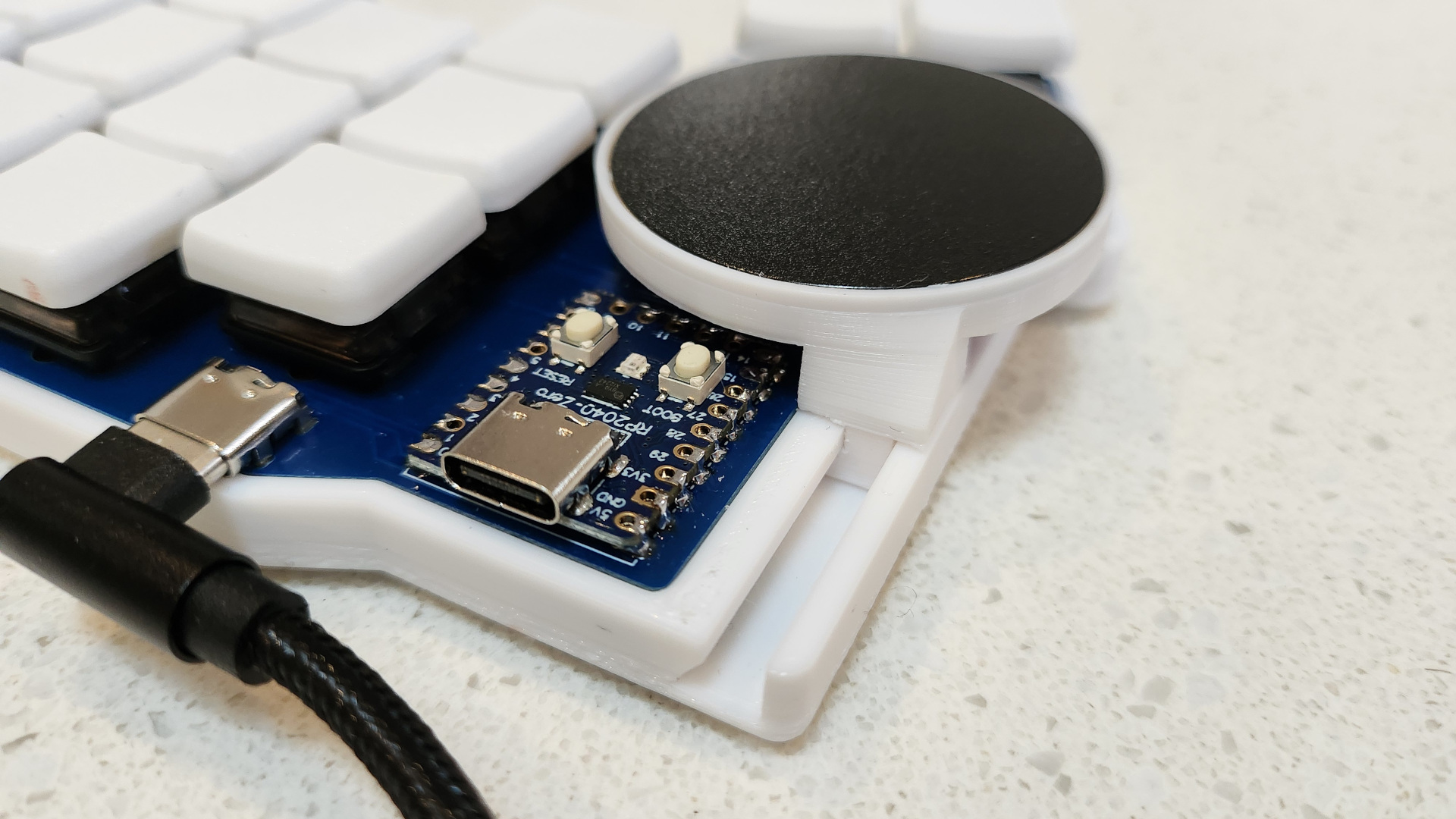
The .stls are in the printables folder and there is also the OnShape Project in case you want to make modifications.
| Qty | Value | Footprint | References |
|---|---|---|---|
| 32 | PG1350 | S1, S2, S10, S11, S12, S13, S14, S15, S16, S17, S18, S19, S20, S21, S22, S23 +16 | |
| 32 | ComboDiode | D1, D2, D10, D11, D12, D13, D14, D15, D16, D17, D18, D19, D20, D21, D22, D23 +16 | |
| 6 | MountingHole_2.2mm_M2_Pad_Via | _1, _2, _3, _4, _5, _6 | |
| 2 | RP2040-Zero | RP2040Zero1, RP2040Zero2 | |
| 2 | LOGO | Aafootprints:logo | G***, G*** |
| 2 | LOGO | Aafootprints:url | G***, G*** |
| 1 | LOGO | Aafootprints:wing-right-large | G*** |
| 1 | LOGO | Aafootprints:wing-left | G*** |
| 1 | LOGO | Aafootprints:wing-right | G*** |
| 1 | LOGO | Aafootprints:wing-left-large | G*** |
The 80 most common of 84 parts.

pcbreflux/espressif
all espressif stuff will committed here

CRImier/MyKiCad
My KiCad boards. Can't be bothered uploading individually anymore, so here you go.


Rack-Robotics/Powercore-V1.0-Hardware
CAD & Electronics for Powercore V1

esp-cpp/esp-box-emu
Star Wars: Dark Forces, Doom, NES, Gameboy/Color, Sega Master System / GameGear, Sega Genesis / MegaDrive, and MSX I/II Emulators running on ESP BOX and ESP BOX-3 with a custom gamepad


Redherring32/OpenTendo-TopLoader
An Open Source HardWare (OSHW) recreation of the 1993 toploading NES motherboard (Also known as NES-101)
It measures 262.6 × 94.4 mm and has 2 copper layers, 1.6 mm thick.
84 parts. The full list of its parts is on this page, with links to each part's symbol and footprint where PCBKit's library has them.
From the dlip/tenshi repository on GitHub, at the commit this page was made from: the board is kicad/tenshi.kicad_pcb. PCBKit opens the board in the browser, with nothing to install.
Its repository publishes it under the GPL-3.0 licence: you may reuse it on that licence's terms (keep the author's notice, and for a copyleft licence share your changes alike).