4 layers53 × 39 mm
Avclan mockingboard rounded
halleysfifthinc/AVCLAN-Mockingboard
Emulate a CD Changer on a Toyota AVC LAN network
43 parts65GPL-3.0

 DJM0/LoadShed1
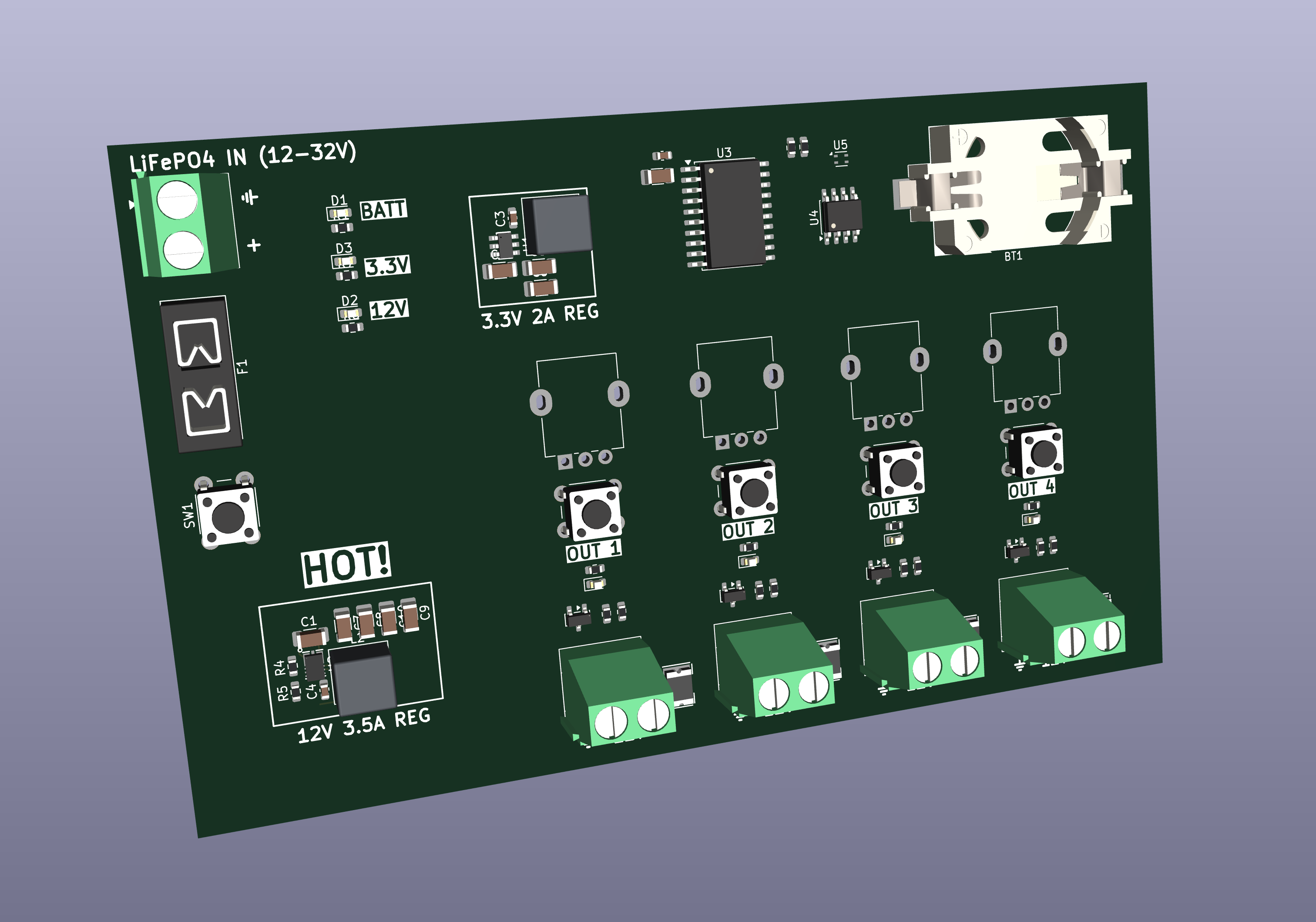
Off-grid 4-channel PWM load controller with regulated 12 V output from any 12–32 V battery. Sunrise/sunset + RTC scheduling, LiFePO₄ battery protection, dimming pots and an OLED. ATtiny3216 firmware + KiCad hardware. No WiFi, no cloud, no app.
LoadShed is an open-source printed circuit board by DJM0, from the DJM0/LoadShed repository on GitHub, published under the MIT licence. It is a 2-layer board of 151.2 × 89.3 mm with 94 parts on 56 nets, routed with 345 tracks and 72 vias.
It is built around the ATTINY3216-SF, DS3231MZ/V+ and AO3400A, with the BS-06-B4AA002 among its other parts. Its parts include 24 resistors, 18 capacitors, 14 connectors, 7 diodes and 6 fuses. It belongs with the power and radio and wireless boards and the AVR (ATmega, ATtiny) boards of this library.


KiCad 9 project for the LoadShed PCB. Licensed under CERN-OHL-P v2.
loadshed.kicad_pro / .kicad_sch / .kicad_pcb   KiCad 9 project
loadshed-schematic.pdf                         Schematic export (browse without KiCad)
sym-lib-table / fp-lib-table                   Project library tables (see JLCImport note)
fabrication-toolkit-options.json               Fabrication Toolkit settings (JLCPCB)
production/
  gerbers_v1.2.zip                             Gerbers as fabricated (v1.2)
  bom.csv                                      BOM with LCSC part numbers
  positions.csv / designators.csv              Pick-and-place files
  netlist.ipc                                  IPC netlist
bom/ibom.html Interactive HTML BOMSeveral parts (regulators, inductors, polyfuses, battery holder, buttons…)
were pulled from JLCPCB/LCSC using the
kicad-jlcimport plugin,
which converts EasyEDA CAD data into a project-local JLCImport library.
Because that converted data comes from EasyEDA/LCSC, its redistribution
licence is unclear, so the JLCImport symbol/footprint/3D-model libraries
are not included in this repo.
This matters less than it sounds:
.kicad_sch and every
footprint in the .kicad_pcb, so the project opens, edits, and fabricates
fine without the libraries. Expect harmless "library not found" /
"footprint not found in library" warnings in ERC/DRC, and missing 3D models
for those parts in the 3D viewer.production/bom.csv. The
plugin recreates JLCImport.kicad_sym, JLCImport.pretty/ and
JLCImport.3dshapes/ in the project directory, where the committed
sym-lib-table / fp-lib-table already point.
(easyeda2kicad is a CLI
alternative that does the same conversion.)The silkscreen says LiFePO₄ IN (12–32 V). The technical ceiling is set by the smaller regulator: the AP63203 3.3 V buck accepts 3.8–32 V (the AP64502 12 V buck is good to 40 V). Two caveats above ~15 V:
VBAT_DIVIDER in the firmware's config.h.Candid notes for anyone considering a respin:
For the record, v1.2 fits all of its designer's needs and there was never a reason for a second spin. A v2 wishlist, should anyone take one on: one or two dry-contact relay channels, per-channel clamping, input reverse-polarity protection, and selectable output sourcing (unregulated battery through the MOSFETs, or additional regulated rails such as 5 V routable to a channel).
Costs, assembly details and the offer of at-cost boards live in the main README. The mechanics:
production/ were generated with the
Fabrication Toolkit
KiCad plugin (settings committed in fabrication-toolkit-options.json).bom.csv carries LCSC part numbers for every placed part; JLCPCB economic
assembly places all SMD parts from it.bom/ibom.html in a browser for an interactive placement view.| Qty | Value | Footprint | References |
|---|---|---|---|
| 7 | 100nF | Capacitor_SMD:C_0603_1608Metric | C1, C3, C4, C7, C11, C13, C14 |
| 7 | LED | LED_SMD:LED_0603_1608Metric | D1, D2, D3, D4, D5, D6, D7 |
| 6 | 100K | Resistor_SMD:R_0603_1608Metric | R4, R8, R11, R14, R17, R20 |
| 5 | 1K | Resistor_SMD:R_0603_1608Metric | R7, R10, R13, R16, R19 |
| 5 | Polyfuse | JLCImport:1812L300_24SLER | F2, F3, F4, F5, F6 |
| 4 | 100R | Resistor_SMD:R_0603_1608Metric | R9, R12, R15, R18 |
| 4 | 10uF | Capacitor_SMD:C_1206_3216Metric | C2, C12, C15, C21 |
| 4 | 47uF | Capacitor_SMD:C_1210_3225Metric | C16, C17, C18, C19 |
| 4 | AO3400A | Package_TO_SOT_SMD:SOT-23 | Q1, Q2, Q3, Q4 |
| 4 | Conn_01x03_Socket | Connector_PinHeader_2.54mm:PinHeader_1x02_P2.54mm_Vertical | J10, J11, J12, J13 |
| 4 | MountingHole | MountingHole:MountingHole_3.2mm_M3_DIN965_Pad | H1, H2, H3, H4 |
| 4 | R_Potentiometer | Potentiometer_THT:Potentiometer_Alpha_RD901F-40-00D_Single_Vertical | RV1, RV2, RV3, RV4 |
| 4 | SW_Push | Button_Switch_THT:SW_PUSH_6mm | SW3, SW4, SW5, SW6 |
| 2 | 22uF | Capacitor_SMD:C_1206_3216Metric | C5, C6 |
| 2 | 27K | Resistor_SMD:R_0603_1608Metric | R5, R21 |
| 2 | 4K7 | Resistor_SMD:R_0603_1608Metric | R2, R3 |
| 2 | 6K8 | Resistor_SMD:R_0603_1608Metric | R1, R6 |
| 2 | OUT4 | TerminalBlock_Phoenix:TerminalBlock_Phoenix_MKDS-1,5-2-5.08_1x02_P5.08mm_Horizontal | J5, J7 |
| 1 | 10K | Resistor_SMD:R_0603_1608Metric | R23 |
| 1 | 10nF | Capacitor_SMD:C_0603_1608Metric | C20 |
| 1 | 140K | Resistor_SMD:R_0603_1608Metric | R22 |
| 1 | 200K | Resistor_SMD:R_0603_1608Metric | R24 |
| 1 | 4.7µH | JLCImport:0630CDMCCDS-4R7MC | L1 |
| 1 | 5A | Fuse:Fuseholder_Blade_Mini_Keystone_3568 | F1 |
| 1 | 6.8µH | JLCImport:0630CDMCCDS-6R8MC | L3 |
| 1 | AP63203WU-7 | JLCImport:AP63203WU-7 | U1 |
| 1 | AP64502QSP-13 | JLCImport:AP64502QSP-13 | U6 |
| 1 | ATtiny3216-S | Package_SO:SOIC-20W_7.5x12.8mm_P1.27mm | U3 |
| 1 | BATT | TerminalBlock_Phoenix:TerminalBlock_Phoenix_MKDS-1,5-2-5.08_1x02_P5.08mm_Horizontal | J1 |
| 1 | BS-06-B4AA002 | JLCImport:BS-06-B4AA002 | BT2 |
| 1 | DS3231MZ | Package_SO:SOIC-8_3.9x4.9mm_P1.27mm | U4 |
| 1 | OLED | Connector_PinHeader_2.54mm:PinHeader_1x04_P2.54mm_Vertical | J6 |
| 1 | OLED2 | Connector_PinHeader_2.54mm:PinHeader_1x04_P2.54mm_Vertical | J14 |
| 1 | OUT1 | TerminalBlock_Phoenix:TerminalBlock_Phoenix_MKDS-1,5-2-5.08_1x02_P5.08mm_Horizontal | J2 |
| 1 | OUT2 | TerminalBlock_Phoenix:TerminalBlock_Phoenix_MKDS-1,5-2-5.08_1x02_P5.08mm_Horizontal | J3 |
| 1 | OUT3 | TerminalBlock_Phoenix:TerminalBlock_Phoenix_MKDS-1,5-2-5.08_1x02_P5.08mm_Horizontal | J4 |
| 1 | PB3 | Connector_PinSocket_2.54mm:PinSocket_1x03_P2.54mm_Vertical | J9 |
| 1 | POWER SW | Custom:T8013_ToggleSwitch_SPDT_1 | SW1 |
| 1 | SHT4x | Sensor_Humidity:Sensirion_DFN-4_1.5x1.5mm_P0.8mm_SHT4x_NoCentralPad | U5 |
| 1 | UPDI | Connector_PinSocket_2.54mm:PinSocket_1x03_P2.54mm_Vertical | J8 |
It measures 151.2 × 89.3 mm and has 2 copper layers, 2 mm thick.
94 parts, built around the ATTINY3216-SF, DS3231MZ/V+, AO3400A and BS-06-B4AA002. The full list of its parts is on this page, with links to each part's symbol and footprint where PCBKit's library has them.
From the DJM0/LoadShed repository on GitHub, at the commit this page was made from: the board is hardware/loadshed.kicad_pcb and its schematic hardware/loadshed.kicad_sch. PCBKit opens the board in the browser, with nothing to install.
Its repository publishes it under the MIT licence: you may reuse it on that licence's terms (keep the author's notice, and for a copyleft licence share your changes alike).
halleysfifthinc/AVCLAN-Mockingboard
Emulate a CD Changer on a Toyota AVC LAN network

MichielVanwelsenaere/HomeAutomation.ModbusRtuSensorHub
PCB with small footprint designed to act as a Modbus RTU slave.


alexanderenrique/smart_tbird
Smart Thunderbird vehicle electronics — ESP32 nodes, alternator delay, display, and tooling.


gugray/InterGalacticReceiver
Tune in to alien transmissions on a CRT screen! Shaders are involved.
