
2 layers40 × 20 mm

Six-key XIAO RP2040 Hackpad: KiCad PCB, Fusion case, CircuitPython firmware and desktop helper. AI-assisted design prototype; integration testing in progress.
Hackpad is an open-source printed circuit board by DillGrammer, from the DillGrammer/school-creator-hackpad repository on GitHub. It is a 2-layer board of 86.5 × 88.5 mm with 13 parts on 14 nets, routed with 143 tracks and 2 vias.
Its parts include 7 switches, 1 IC and 1 connector. It belongs with the RP2040 boards of this library.
Open Hackpad.kicad_pro in KiCad 10. The project includes its own symbol and footprint libraries; no care-package installation is needed. Original Desktop files were left unchanged.
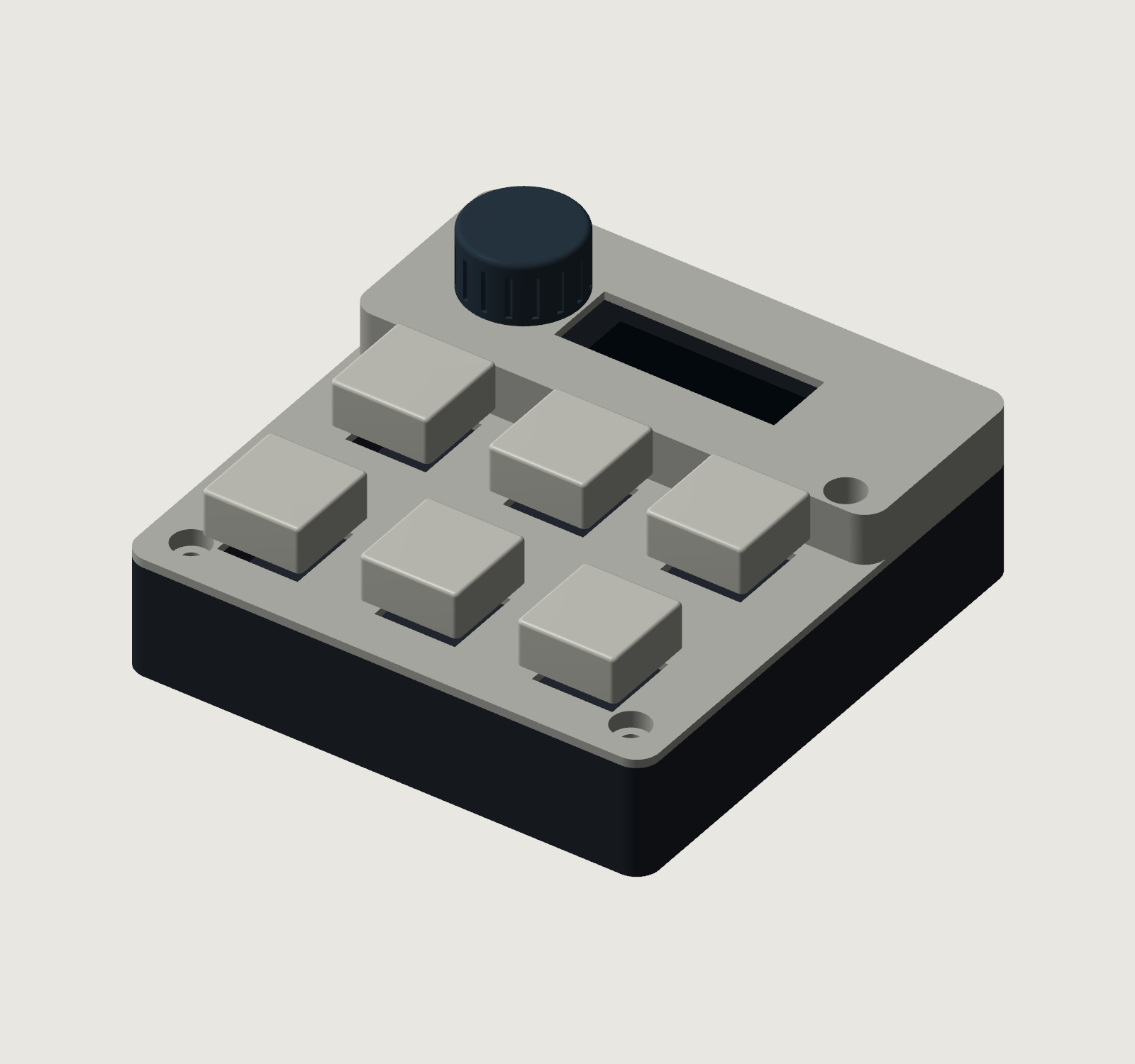
CAD visualization, not a photograph of an assembled device.
This project was substantially generated and revised with ChatGPT/Codex assistance, following the owner's feature/layout choices and design review. See Software/Feature-status.md for unfinished integrations and Submission-status.md for funding status.
The matching case is supplied in Case/ as STEP and STL files, with an assembly guide and geometry checks. The native Fusion Case/Hackpad_Case.f3d includes editable base/cover features and a positioned knob. Case revision 1.1 corrects the CAD Y direction and knob placement; use the new case files, not earlier archives. Actual firmware and desktop-helper source are included in Software/; this is a development build, not a hardware-tested release. See Software/Feature-status.md for the exact remaining integration work.
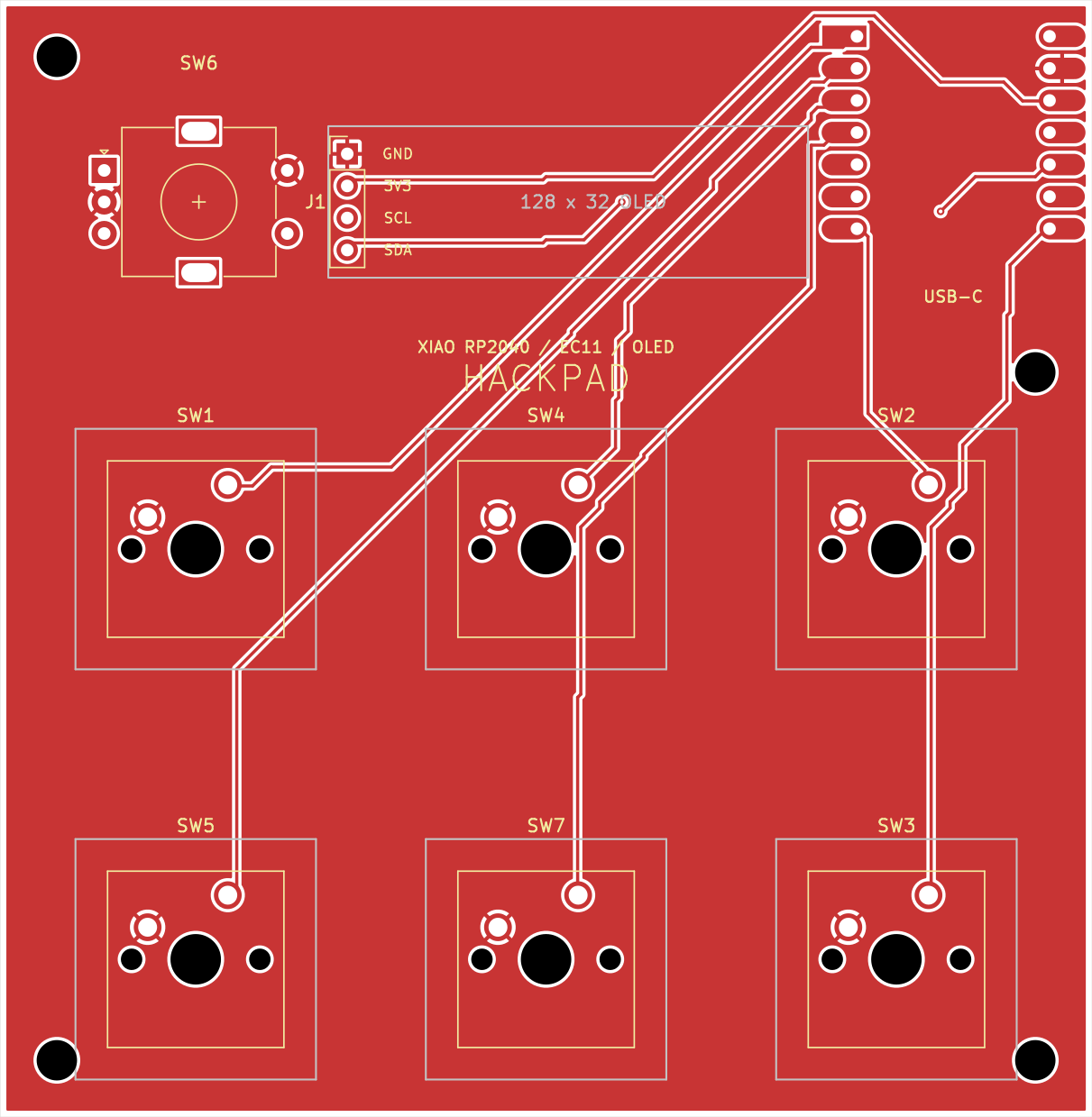
View from above, USB-C at the top. Key numbers describe physical positions; existing SW references are preserved.
| Control | Reference / pad | XIAO label | RP2040 GPIO | Net |
|---|---|---|---|---|
| Top-left key | SW1 / 1 | D0 | 26 | KEY1 |
| Top-middle key | SW4 / 1 | D2 | 28 | KEY2 |
| Top-right key | SW2 / 1 | D6 | 0 | KEY3 |
| Bottom-left key | SW5 / 1 | D1 | 27 | KEY4 |
| Bottom-middle key | SW7 / 1 | D3 | 29 | KEY5 |
| Bottom-right key | SW3 / 1 | D7 | 1 | KEY6 |
| Encoder rotation A | SW6 / A | D10 | 3 | ENC_A |
| Encoder rotation B | SW6 / B | D9 | 4 | ENC_B |
| Encoder press / Enter | SW6 / S1 | D8 | 2 | ENC_CLICK |
| OLED data | J1 / 4 | D4 / SDA | 6 | OLED_SDA |
| OLED clock | J1 / 3 | D5 / SCL | 7 | OLED_SCL |
| OLED power | J1 / 2 | 3V3 | — | +3V3 |
| OLED ground | J1 / 1 | GND | — | GND |
All key pad 2 connections, encoder C, and encoder S2 connect to ground. Enable input pull-ups and software debounce for keys and encoder press. Use a quadrature decoder for rotation; configure its transitions-per-detent for the supplied encoder so one detent produces one menu step. Reverse direction in firmware if needed. Encoder press is independently wired and can mean Enter/select or another action by mode.
Six keys + three encoder inputs + two OLED signals use all 11 exposed GPIOs. Independent key wiring supports simultaneous presses without a switch matrix or diodes. Extra kit LEDs are not fitted in this design.
| Quantity | Part |
|---|---|
| 1 | Standard Seeed Studio XIAO RP2040, not RP2040 Plus |
| 6 | MX-style through-hole switches |
| 6 | 1u DSA keycaps |
| 1 | EC11 clickable rotary encoder |
| 1 | 0.91-inch 128 × 32 I²C OLED, GND–VCC–SCL–SDA |
| 1 | 4-pin 2.54 mm header supplied with/for OLED |
| 4 | M3 × 16 mm case screws, for planned enclosure |
| 4 | M3 heat-set inserts, for planned enclosure |
Millimetres from PCB top-left; X right, Y down.
| Item | X | Y |
|---|---|---|
| Key column centres | 15.50 / 43.25 / 71.00 | — |
| Key row centres | — | 43.50 / 76.00 |
| Encoder shaft centre | 15.75 | 16.00 |
| OLED GND header pin | 27.50 | 12.19 |
| XIAO footprint centre | 75.50 | 10.50 |
| Mount H1 | 4.50 | 4.50 |
| Mount H2 | 82.00 | 29.50 |
| Mount H3 | 4.50 | 84.00 |
| Mount H4 | 82.00 | 84.00 |
The matching case uses a rounded base and removable stepped cover, four M3 screws and heat-set inserts. See Case/Assembly-guide.md for the assembly order, printing orientation and component fit assumptions.
Use the Gerbers ZIP, including both drill files, for the PCB only. Board specification: two layers, FR-4, 1.6 mm thickness; design uses 0.25 mm traces, 0.20 mm minimum clearance, 0.60/0.30 mm vias, and 0.50 mm minimum copper-to-edge clearance. The Stardance design project has been created; no funding application or manufacturing order has been submitted. See Submission-status.md.
The checks validate the CAD files; this design has not been physically assembled or tested. The case has CAD checks but no physical print test; software has automated logic/display tests but still requires hardware and app integration testing.
Footprints are derived from KiCad's installed libraries and the user's existing Hackpad care package. The XIAO's fabrication graphics were retained, and its courtyard added. The OLED header footprint was expanded to describe the full module envelope.
| Qty | Value | Footprint | References |
|---|---|---|---|
| 6 | MX_Switch | Hackpad:SW_Cherry_MX_1.00u_PCB | SW1, SW2, SW3, SW4, SW5, SW7 |
| 4 | MountingHole | Hackpad:MountingHole_3.2mm_M3 | H1, H2, H3, H4 |
| 1 | EC11_Click | Hackpad:RotaryEncoder_Alps_EC11E-Switch_Vertical_H20mm | SW6 |
| 1 | OLED_128x32 | Hackpad:OLED_091_GND_VCC_SCL_SDA | J1 |
| 1 | XIAO_RP2040 | Hackpad:XIAO-Generic-Hybrid-14P-2.54-21X17.8MM | U1 |
It measures 86.5 × 88.5 mm and has 2 copper layers, 1.6 mm thick.
13 parts. The full list of its parts is on this page, with links to each part's symbol and footprint where PCBKit's library has them.
From the DillGrammer/school-creator-hackpad repository on GitHub, at the commit this page was made from: the board is Hackpad.kicad_pcb and its schematic Hackpad.kicad_sch. PCBKit opens the board in the browser, with nothing to install.
Its repository states no licence, so its author keeps all rights: ask DillGrammer before reusing the design.


samyk/magspoof
A portable device that can spoof/emulate any magnetic stripe, credit card or hotel card "wirelessly", even on standard magstripe (non-NFC/RFID) readers.

fossasia/pslab-scripts
Pocket Science Lab - Scripts for Sensor Experiments


willem-pennings/balancing-cube
A cube that balances itself in a corner or edge using reaction wheels

VoronDesign/Voron-Hardware
Cool Hardware designed by the Voron Design group

hoglet67/RGBtoHDMI
Bare-metal Raspberry Pi project that provides pixel-perfect sampling of Retro Computer RGB/YUV video and conversion to HDMI