2 layers98 × 27 mm

 defparam/PCI2Nano-PCB32
An FPGA/PCI Device Reference Platform
Pci2nano is an open-source printed circuit board by defparam, from the defparam/PCI2Nano-PCB repository on GitHub, published under the CC-BY-SA-4.0 licence. It is a 2-layer board of 79.2 × 69.2 mm with 5 parts on 99 nets, routed with 807 tracks and 123 vias.
It belongs with the fPGA and programmable logic boards of this library.
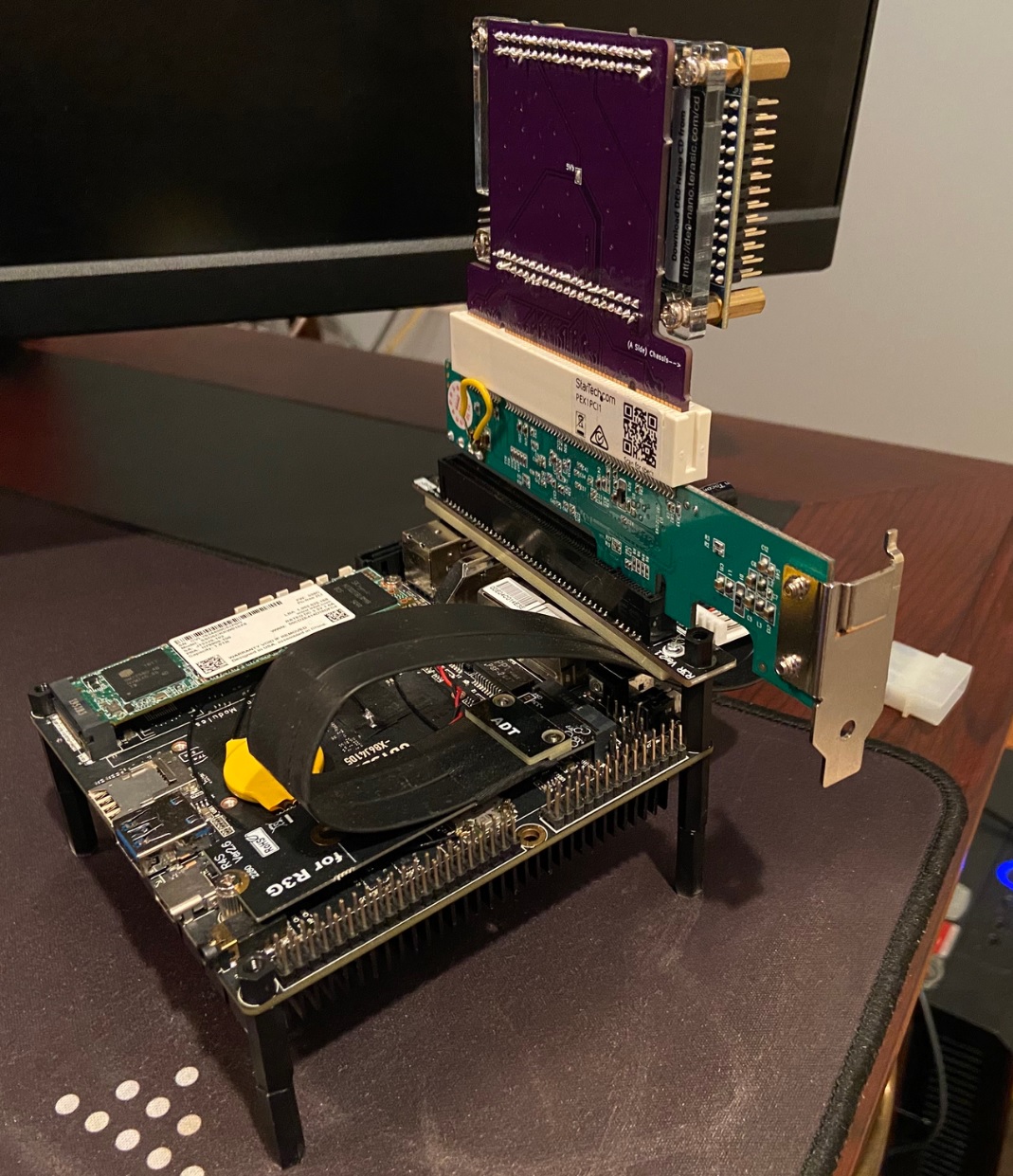
Welcome to the PCI2Nano Reference Platform repo. In this repo you'll find an inexpensive suggested Reference Platform for designing and testing PCI functions on a DE0-Nano FPGA to an x86 host. I have personally built/connected/tested every single one of these components and can confirm they work for fast iterative PCI development.
The design collateral that is included with this repo are the kicad design files for the PCI2Nano breakout board and a Quartus project that contains all the correct PCI pinout constraints for the PCI2Nano breakout board. This repo does not contain an actual PCI core written in verilog. For an example PCI core implementation with a UART check out the PCI2Nano-RTL repo here: https://github.com/defparam/PCI2Nano-RTL/

This work is licensed under a Creative Commons Attribution-ShareAlike 4.0 International License.
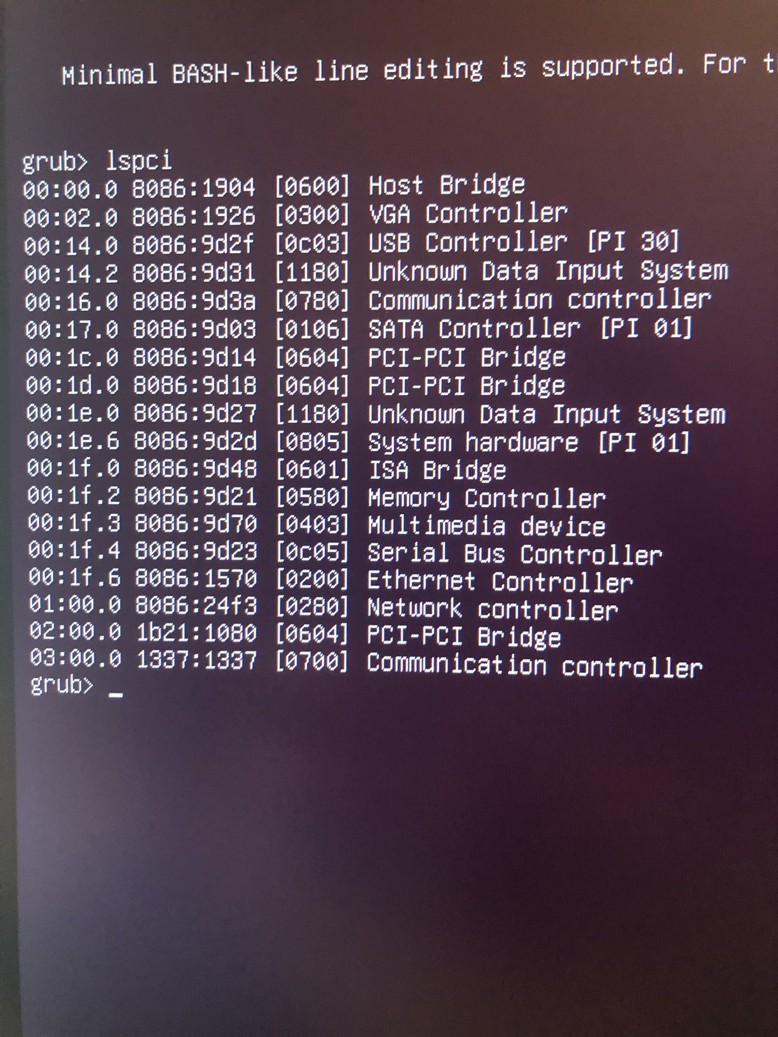
My l337-Communication Controller
| Part | Description | Price |
|---|---|---|
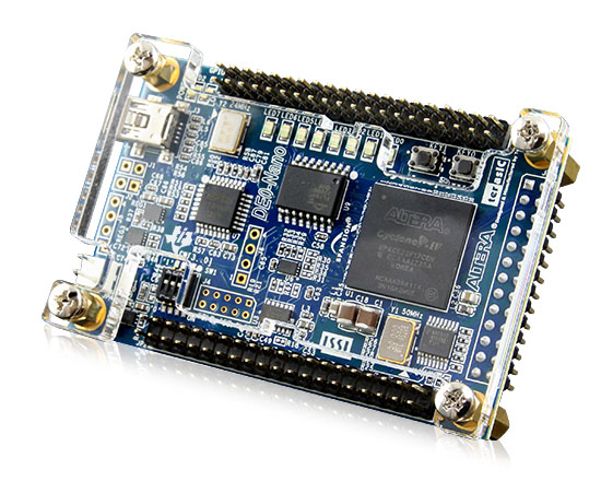
| DE0-Nano | FPGA Board | ~$100.00 |
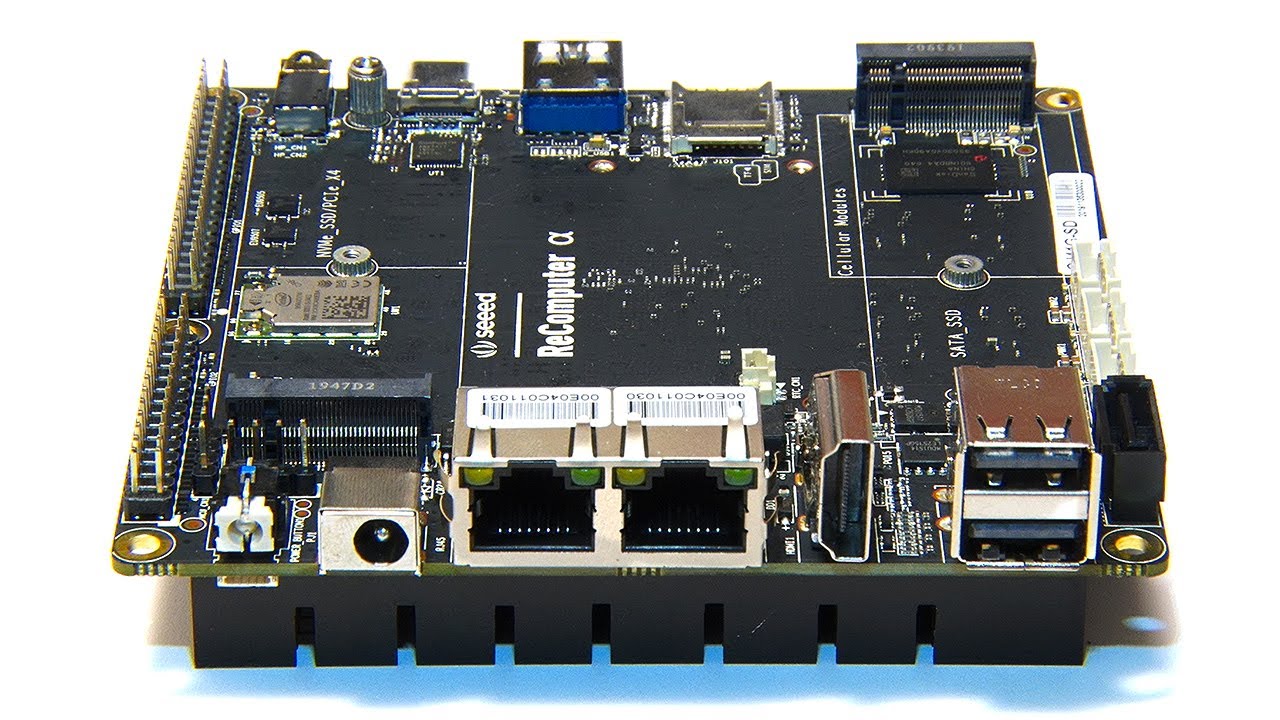
| Seeed Odyssey X86J4105 SBC | SIngle Board Computer | ~$185.00 |
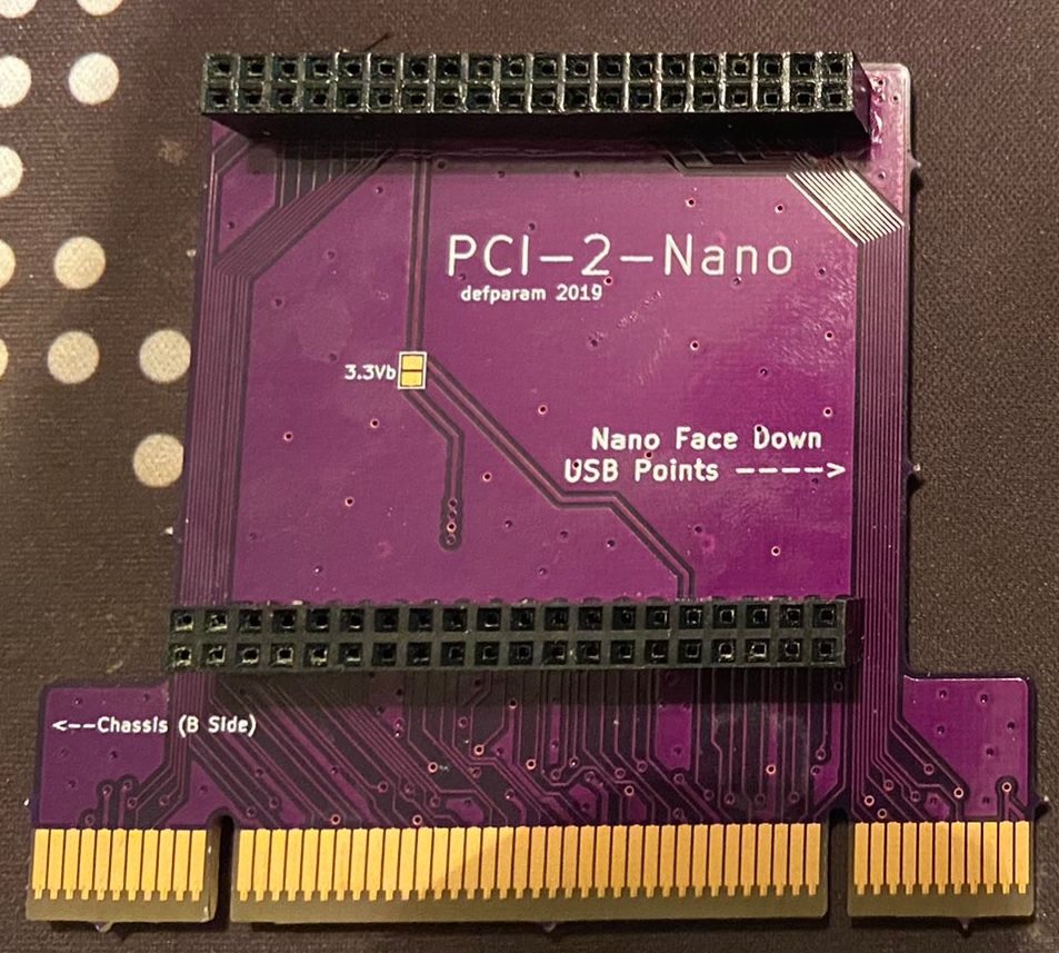
| PCI2Nano Breakout PCB | Coverts PCI to DE0-Nano GPIO | ~$45 (OSHPark for 3) |
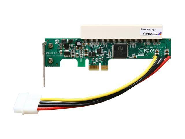
| Startech PEX1PCI1 | Converts PCIe to PCI | ~$40 |
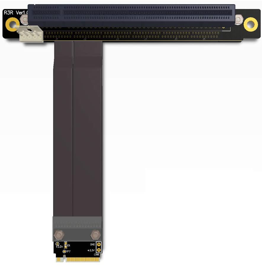
| M.2 Key M Extender PCIE x16 | Break out M.2 to PCIe x16 | ~$32 |
| 2x 100mil 40-pin IDC sockets | Soldered to the PCB | ~$1-$2 |
There is a small amount of soldering involved with the PCB board to connect the 100mil IDC socket to the PCB board.
The DE0-Nano:
The PCI2Nano PCB:
The PEX1PCI1 PCIe-2-PCI Bridge:
The Seeed Odyssey X86J4105 SBC:
The M.2 Key M Extender PCIE x16:
| Qty | Value | Footprint | References |
|---|---|---|---|
| 2 | Conn_02x20_Odd_Even | Connector_PinHeader_2.54mm:PinHeader_2x20_P2.54mm_Vertical | J2, J3 |
| 2 | SolderJumper_2_Bridged | Jumper:SolderJumper-2_P1.3mm_Open_Pad1.0x1.5mm | JP1, JP2 |
| 1 | Bus_PCI_32bit_Universal | Connector_PCBEdge:BUS_PCI_UNIVERSAL_edgecuts | J1 |
It measures 79.2 × 69.2 mm and has 2 copper layers, 1.6 mm thick.
5 parts. The full list of its parts is on this page, with links to each part's symbol and footprint where PCBKit's library has them.
From the defparam/PCI2Nano-PCB repository on GitHub, at the commit this page was made from: the board is pci2nano.kicad_pcb. PCBKit opens the board in the browser, with nothing to install.
Its repository publishes it under the CC-BY-SA-4.0 licence: you may reuse it on that licence's terms (keep the author's notice, and for a copyleft licence share your changes alike).

joypad-ai/joypad-os
Universal controller firmware for building adapters, dongles, and custom controllers.

OLIMEX/OLINUXINO
OLINUXINO is Open Source / Open Hardware, low cost from EUR 24 Linux Industrial grade Single Board Computer capable to operate -25+85C

jamro/tiny-engineer
A small desktop robot that brings an AI coding assistant to life, physically acting out when it reads files, thinks, writes code, and finishes work.

hackclub/OnBoard
💡 Join 1,000 teenagers and make your first PCB with a $100 grant!


Luos-io/luos_engine
Open-source and real-time orchestrator for cyber-physical-systems, to easily design, test and deploy embedded applications and digital twins.