2 layers20.5 × 24.8 mm

 DD-stella/Learning-KiCad-Projects
從零開始的 KiCad PCB 設計
Project 01 First LED is an open-source printed circuit board by DD-stella, from the DD-stella/Learning-KiCad-Projects repository on GitHub. It is a 2-layer board of 76 × 48.5 mm with 8 parts on 7 nets, routed with 31 tracks and 2 vias.
Its parts include 3 resistors, 2 capacitors, 1 IC, 1 diode and 1 connector.
你好!我是 柯宇鴻,這是用來記錄我從零開始學習 KiCad PCB 設計的 GitHub 倉庫。 我希望藉由實作不同的專案,掌握電路圖設計與 PCB 佈線的技能,為未來的專案打下基礎。
為了掌握系統化的硬體電路設計流程,我將依據標準 SOP 逐步完成以下階段的學習與實作:
✅ 掌握元件庫搜尋與基本元件放置(R, C, IC, Connector)
實作筆記:
- 按下快捷鍵'A'可以搜尋並新增符號
- 將滑鼠移到元件上,按'R'可以旋轉方向、按'M'可以移動。
- 按下快捷鍵'W'可以畫綠色的導線(其實也可以不用按)連接元件接腳,按'Esc'退出。
✅ 理解並正確放置「電源標籤」(Power Flag) 解決電源供應端判定問題
實作筆記:
- ★★★ 雖然在電路圖中放了'+5' 和 'GND',但 KiCad 預設不知道電源是從哪裡「輸入」的,因此直接執行 ERC 會報錯。
- ★★★ 解決方法:按 'A' 搜尋 'PWR_FLAG'(電源標籤)並放置兩個。
- 將其中一個接在 '+5V'和'GND'線路上,藉此告訴系統這兩條是電源源頭。
✅ 執行原理圖「電氣規則檢查」(ERC) 並修正所有 Errors 與 Warnings
實作筆記:
- 點選上方工具列的圖示(ERC)開啟檢查視窗。
- 點擊「執行 ERC」,只要「違規」頁籤顯示為 (0) 即代表完全通過。
✅ 學會閱讀晶片數據手冊 (Datasheet),理解引腳定義與電氣屬性
實作筆記:
- 畫晶片的第一步絕對是查 Datasheet 確認引腳功能(例如 NE555 讓 LED 閃爍的電路中,Pin 1 是 GND、Pin 8 是 VCC、Pin 3 是 OUT)。
- ★★★ 註:如果要參考 Datasheet 的詳細設計與封裝規範,請以 HackMD 講義 網站裡的標準為主。
✅ 實作「自建電路圖符號」(Custom Symbol),手動繪製晶片符號並設定 Pin Type (Input/Output/Power)
實作筆記:
- 建立新圖庫並在「管理符號庫」掛載時,路徑一定要選
${KIPRJMOD}開頭的「相對路徑」!- ★★★ 如果留著
C:\...開頭的絕對路徑,換台電腦或上傳 GitHub 後,系統會去別人的 C 槽找檔案,絕對會大翻車「查無此零件」,而且系統也會查不到。- ★★★在畫晶片接腳(按 'P')時,端點小圓圈要朝外(那是用來接線的)。
- 「電氣類型」一定要照 Datasheet 乖乖選(例如 VCC 和 GND 要選 Power Input)。亂選的話,畫完電路圖按 ERC 會被錯誤訊息淹沒。
✅ 實作「自建封裝」(Custom Footprint),根據 Datasheet 尺寸精密計算焊盤 (Pad) 大小、間距 (Pitch) 與邊界線 (Courtyard)
實作筆記:
- 建立封裝庫一樣要選 '專案(Project)' 層級,確保上傳 GitHub 後路徑不會出錯。
- ★★★ 尺寸計算與格點設定:DIP-8 封裝的引腳間距 (Pitch) 是 2.54mm (100 mil),左右排間距是 7.62mm (300 mil)。可以直接把上方選單的格點改為 '2.5400 mm (100.00 mils)'。這樣放置下一個焊盤時,只要相差一格,距離就絕對精準!
- ★★★ 焊盤(Pad)擺放與編號規則:點選右側的黃色圓圈圖示(加入焊盤)開始打洞
- ★★★ 第一腳防呆設定:滑鼠指著 Pin 1 按鍵盤'E'編輯,將形狀改成'矩形' (其餘 2-8 腳保持圓形)。並在 'F.Silkscreen'(絲印層)用圓形工具畫個小圓點在 Pin 1 旁邊。
- 外框與邊界設計:在 'F.Silkscreen' 用矩形工具畫個框包住 8 個腳;接著★★★ 絕對不能忘記切換到 'F.Courtyard'(邊界線)再畫一個更大的隱形外框!這是零件的防撞結界,沒畫的話 DRC 無法進行碰撞檢查,到時候跟其他零件擠在一起工廠會拒絕生產。
✅ 將原理圖設計正確導入 PCB 編輯器中
實作筆記:
- 在原理圖中按下快捷鍵 'F8' 就可以把零件實體化傳送到 PCB 世界。
- 剛傳過去時零件會黏在滑鼠上,在畫面點一下左鍵就可以把它們放出來。
✅ 在 Edge.Cuts 層定義精確的電路板尺寸與板框
實作筆記:
- ★★★ 畫板框前,右邊圖層一定要切換到 'Edge.Cuts' 層(通常是黃色的)。如果用別層畫,工廠會不知道從哪裡切板子!
- 選好圖層後,使用右側的「繪製矩形」工具在零件周圍畫一個框,這就是板子的邊界(點兩下可以修改長寬)。
✅ 設定符合生產工廠規範的「設計規則」(Constraints / Design Rules)
實作筆記:
- 預設的 '0.2mm' 線寬太細了,工廠做出來可能會斷掉。
- ★★★ 解決方法:在左上角線寬選單點選「編輯預定義尺寸」,新增一個 '0.4mm' 尺寸並選用它。
✅ 執行「設計規則檢查」(DRC) 確保板子無任何短路、斷路或間距衝突
實作筆記:
- 按下快捷鍵'X'可以開始拉線(F.Cu紅色的那一層)。
- ★★★ 把所有白色的飛線都拉成紅色的實體導線後,點擊上方圖示(ERC)執行檢查。
✅ 實作去耦電容 (Decoupling Capacitor)「盡量靠近晶片電源腳」的佈局規範
實作筆記:
- ★★★ 去耦/濾波電容(如 C2)一定要貼死在晶片對應的引腳旁邊(Pin 5)!
- 這是因為高頻雜訊很敏感,只要導線拉長一點點,電容直接當場廢掉。
- 佈線時,所有的 GND 飛線通通不准用手拉。
- ★★★ 預留秘密武器:下一動要用「大面積鋪銅」,讓所有的 GND 自動接通。
✅ 執行「設計規則檢查」(DRC) 確保板子無任何短路、斷路或間距衝突
實作筆記:
- 按下快捷鍵'X'可以開始拉線(F.Cu紅色的那一層)。
- ★★★ 把所有白色的飛線都拉成紅色的實體導線後,點擊上方圖示(ERC)執行檢查。
- 舖完銅之後,點擊上方圖示(DRC)執行檢查,只要違規與未連線項目都顯示為 (0) 就算完美通關!
✅ 透過 3D 檢視器(3D Viewer)進行機構防撞與高度驗證,並導出高解析度 3D 渲染圖
實作筆記:
- 按下快捷鍵 'Alt+3' 可以開啟 3D 查看器。
- ★★★ 機構驗證重點:不只是好看,更重要的是在送去工廠前,確認電感、電容、排針實體高度會不會跟板框或外殼卡到(進行機構干涉檢查)。
如果有更新原圖,可以按圖是(更新PCB進行放置新元件)
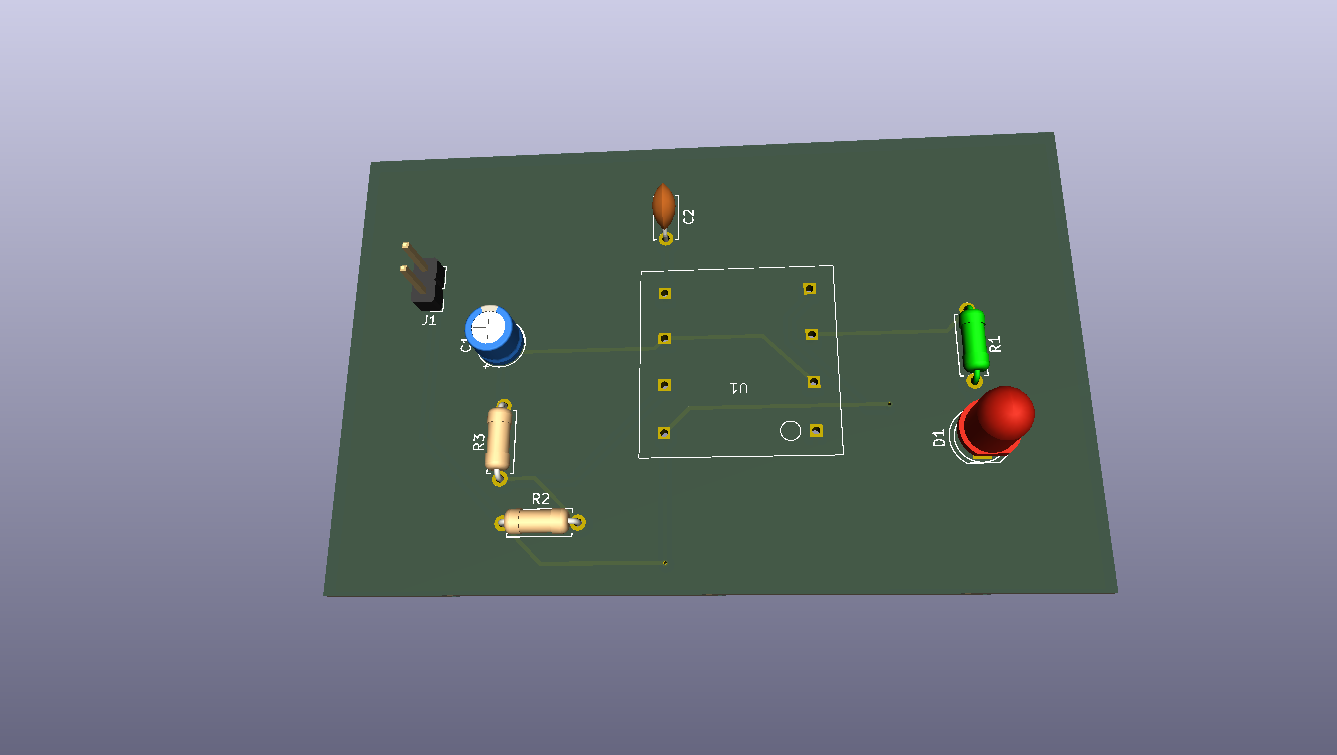 ↑第一個作品↑
✅ 導出符合工廠打樣標準的 Gerber 光繪檔與鑽孔檔 (Drill files)
實作筆記:
- ★★★ 導出路徑建議:不要直接丟在專案根目錄,新建一個叫 'Gerber' 的資料夾來放,不然上百個製造檔會把 GitHub 塞爆。
- 在 PCB 編輯器點選「檔案」->「製造輸出」->「Gerber」,勾選必備圖層 (F.Cu、B.Cu、F.Silkscreen、B.Silkscreen、F.Mask、B.Mask、Edge.Cuts)。
- 點選「繪製(Plot)」生成光繪檔;接著點選「產生鑽孔檔」生成孔位數據,缺一不可!
✅ 使用 Gerber 查看器 (Gerber Viewer) 進行出廠前自主檢查
實作筆記:
- 這是 DFM(可製造性設計)的精髓。在送交工廠前,必須用 KiCad 主畫面的 'Gerber 查看器' 開啟剛導出的所有檔案。
- ★★★ 自檢重點:確認文字(Silkscreen)有沒有疊在焊盤上、孔位(Drill)有沒有偏心、板框(Edge.Cuts)是不是閉合的。
✅ 輸出完整的物料清單 (BOM 表)
實作筆記:
- BOM 表就是零件採購清單。
- 在原理圖編輯器點選「工具」->「產生 BOM」,導出一個 CSV 格式的檔案。
- ★★★ 採購核對重點:確認元件的阻值、容值、封裝規格(如 DIP-8)都有寫清楚,到時候去電子材料行買零件才不會買錯。
| Qty | Value | Footprint | References |
|---|---|---|---|
| 1 | 0.1uF | Capacitor_THT:C_Disc_D5.0mm_W2.5mm_P5.00mm | C2 |
| 1 | 10k | Resistor_THT:R_Axial_DIN0207_L6.3mm_D2.5mm_P7.62mm_Horizontal | R3 |
| 1 | 10uF | Capacitor_THT:CP_Radial_D5.0mm_P2.00mm | C1 |
| 1 | 1k | Resistor_THT:R_Axial_DIN0207_L6.3mm_D2.5mm_P7.62mm_Horizontal | R2 |
| 1 | 220 | Resistor_THT:R_Axial_DIN0207_L6.3mm_D2.5mm_P7.62mm_Horizontal | R1 |
| 1 | Conn_01x02_Pin | Connector_PinHeader_2.54mm:PinHeader_1x02_P2.54mm_Vertical | J1 |
| 1 | LED | LED_THT:LED_D5.0mm | D1 |
| 1 | ~ | My_IC_Footprints:MY_DIP-8 | U1 |
It measures 76 × 48.5 mm and has 2 copper layers, 1.6 mm thick.
8 parts. The full list of its parts is on this page, with links to each part's symbol and footprint where PCBKit's library has them.
From the DD-stella/Learning-KiCad-Projects repository on GitHub, at the commit this page was made from: the board is 20260711Project_01_First_LED/Project_01_First_LED/Project_01_First_LED.kicad_pcb and its schematic 20260711Project_01_First_LED/Project_01_First_LED/Project_01_First_LED.kicad_sch. PCBKit opens the board in the browser, with nothing to install.
Its repository states no licence, so its author keeps all rights: ask DD-stella before reusing the design.

joeycastillo/Sensor-Watch
A board replacement for the classic Casio F-91W wristwatch

rusefi/rusefi
rusefi - GPL internal combustion engine control unit

hoglet67/RGBtoHDMI
Bare-metal Raspberry Pi project that provides pixel-perfect sampling of Retro Computer RGB/YUV video and conversion to HDMI

shanteacontrols/OpenDeck
A platform for building interactive control and sensing devices using MIDI and OSC built with Zephyr RTOS.

hackclub/OnBoard
💡 Join 1,000 teenagers and make your first PCB with a $100 grant!

dangiu/PicoMemcard
Emulating PSX Memory Card (or controller) using a Raspberry Pi Pico

OLIMEX/DIY-LAPTOP
Do It Yourself Open Source Hardware and Software Modular Hacker's Friendly Laptop