2 layers158 × 11 mm
Daylight Matchstick
VoronDesign/Voron-Hardware
Cool Hardware designed by the Voron Design group
22 parts1.1kGPL-3.0

 David-EIPI/battery-sensor-nrf52840
PCB shared between several wireless sensors based on NRF52840 and powered by 18650 batteries
Battery sensor is an open-source printed circuit board by David-EIPI, from the David-EIPI/battery-sensor-nrf52840 repository on GitHub, published under the BSD-2-Clause licence. It is a 2-layer board of 93.5 × 74.5 mm with 22 parts on 28 nets, routed with 260 tracks and 0 vias.
Its parts include 10 connectors, 2 resistors, 1 capacitor, 1 IC and 1 switch. It belongs with the sensors and measurement and power boards and the AVR (ATmega, ATtiny) boards of this library.
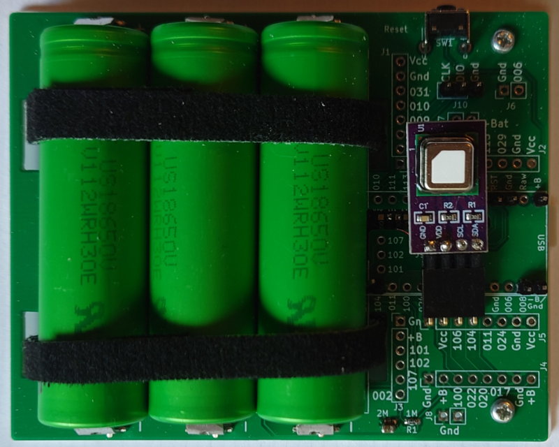
This repository contains a reusable carrier board for battery-powered wireless sensors based on an nRF52840 Pro Micro-style module. It provides space for three 18650 cells, labelled sensor headers, a reset button, SWD programming access, and mounting features for a compact ventilated enclosure. Possible applications include air-quality, environmental, and presence sensors that report to Home Assistant through suitable firmware and a supported wireless protocol.
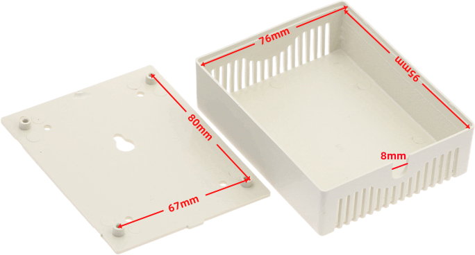
The PCB is designed for the widely available nominal 100 × 80 × 30 mm ventilated plastic enclosure sold by various AliExpress, Amazon, and eBay vendors.
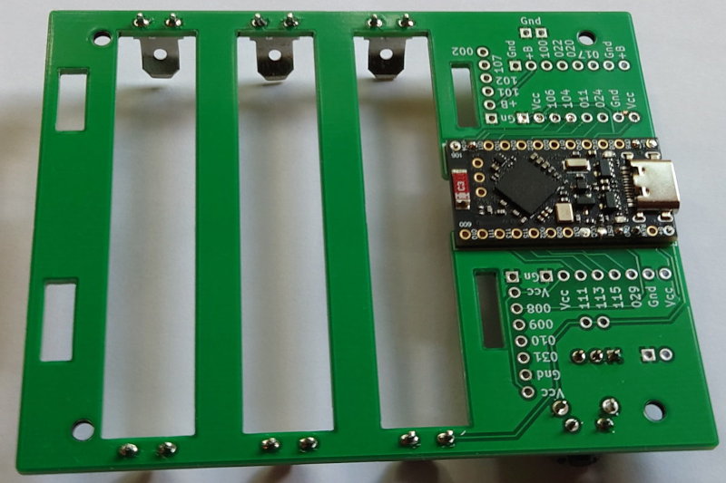
The carrier was designed around the Tenstar Robot ProMicro nRF52840. Although this module resembles the nice!nano, the locations of its extra P1.01, P1.02, and P1.07 pads and its bottom-side SWD pads differ. Check the footprint and pinout carefully before substituting another Pro Micro-style nRF52840 board.
The module's GPIO pins are brought out to 2.54 mm (0.1 inch) headers. The headers also provide ground and either the module's VCC rail or the raw battery rail (+BATT), as marked on the silkscreen. VCC is the module's regulated output; its voltage, current limit, and any software-controlled power switching depend on the particular module fitted (Tenstar module that I have uses 0.5A regulator). The carrier board does not contain its own 3.3 V regulator or load switch.
Pin numbers below run from pin 1 to the last pin of each connector and match the schematic and the square pin-1 pads on the PCB.
| Connector | Pinout |
|---|---|
| J1 | GND, VCC, P0.08, P0.09, P0.10, P0.02, GND, VCC |
| J2 | GND, VCC, P1.11, P1.13, P1.15, P0.29, GND, VCC |
| J3 | GND, +BATT, P1.01, P1.02, P1.07, P0.31 |
| J4 | GND, +BATT, P1.00, P0.22, P0.20, P0.17, GND, +BATT |
| J5 | GND, VCC, P1.06, P1.04, P0.11, P0.24, GND, VCC |
| J6 | GND, P0.06 |
| J7 | +BATT |
| J8 | GND |
| J10 | GND, SWDIO, SWDCLK |
Not every GPIO is an analog input. Consult the nRF52840 datasheet and the fitted module's documentation before assigning sensor signals. The module's RAW pin is not connected on this carrier.
The side-facing push button connects RST to ground. With a compatible UF2/Adafruit-style bootloader installed, a double press normally enters bootloader mode; exact behavior depends on the installed firmware.
The module can normally be updated over USB when its bootloader is working. Hardware debugging and recovery of a damaged or erased bootloader require an SWD probe such as a J-Link.
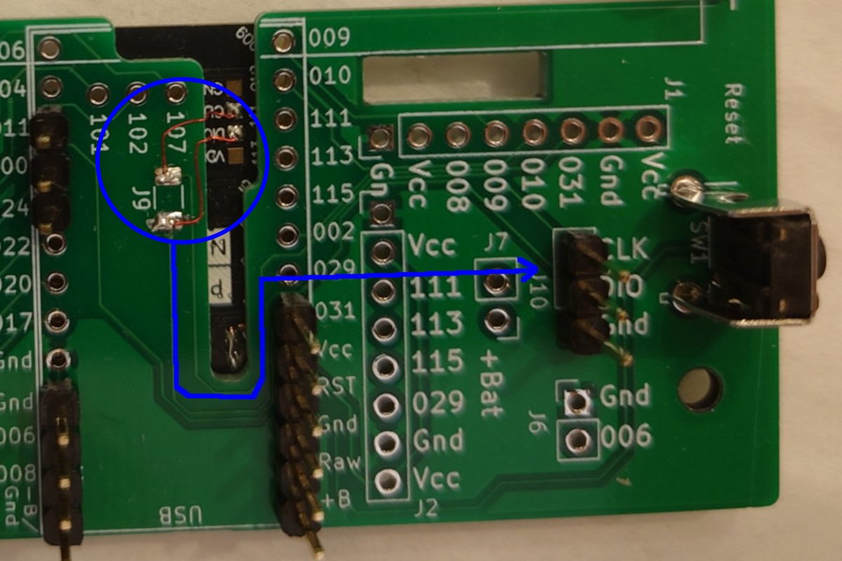
The module's SWDIO and SWDCLK contacts are small pads on its underside. J9 provides two larger landing pads connected to J10. Short jumper wires must be soldered from the module's underside SWD pads to the corresponding J9 pads; J10 then exposes GND, SWDIO, and SWDCLK on a standard 2.54 mm header.
The module is mounted by aligning it with the carrier footprint and soldering through-pins through both boards. Leaving the pins protruding above the module provides convenient test points during development.
The board holds three 18650 lithium-ion cells wired directly in parallel, forming a 1S3P pack. The pack is connected to the module's B+ and B- inputs and is also available on the +BATT headers. The carrier includes no cell-protection, balancing, reverse-polarity, or overcurrent circuitry. USB charging is available only if the fitted module includes a suitable single-cell charger.
Lithium-ion safety: use three identical, healthy cells of the same model, age, capacity, and state of charge. Verify that their voltages are closely matched before installing them in parallel. Observe the marked polarity. Do not rely on this experimental contact arrangement for high-current or unattended applications.
Battery voltage is monitored on P0.31 through a voltage divider (1 MΩ/2 MΩ suggested), so the ADC input is nominally two-thirds of the pack voltage. A 1 µF capacitor is recommended to filter the reading. Firmware must account for the divider ratio, ADC reference, and resistor tolerance when converting the reading to volts.
Standard 18650 holders are generally too long for the enclosure's approximately 74–75 mm internal width. This design instead uses PCB-mounted 6.3 mm blade-tab solder terminals and secures the cells through the PCB slots with cable ties or hook-and-loop straps. The prototype uses TE Connectivity FASTON 250-series PCB tabs with stabilizers; compatible parts are also sold as “6.3 mm lug solder terminals with positioning.” Confirm the exact terminal dimensions against the footprint before ordering.
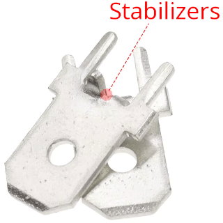
The terminals on the prototype were bent slightly before soldering to improve contact with the ends of the cells. This cell holder is obviosly not intended for high-current applications, but for typical small sensor consumption of less than 0.5A it should suffice.
The two-layer PCB is approximately 93.5 × 74.5 mm and 1.6 mm thick. It has four 3.5 mm mounting holes and 3 slots for securing the cells. The design targets the common ventilated enclosure advertised as 100 × 80 × 30 mm; similar products may also be listed as 100 × 80 × 28 mm or 100 × 80 × 29 mm.
The enclosure has ventilation grilles on two sides, which are useful for environmental sensors. A small opening near the mounting plate aligns with the module's USB-C connector for charging and firmware updates on the prototype enclosure.
The project was created with KiCad 10. The repository contains the editable schematic (battery-sensor.kicad_sch), PCB layout (battery-sensor.kicad_pcb), project settings (battery-sensor.kicad_pro), and Gerber and drill files in gerbers/.
This project is released under the BSD 2-Clause License; see LICENSE.
| Qty | Value | Footprint | References |
|---|---|---|---|
| 4 | MountingHole | MountingHole:MountingHole_3.5mm | H1, H2, H3, H4 |
| 3 | Battery_Cell | my_power:18650-edge-pins | BT1, BT2, BT3 |
| 3 | Conn_01x02_Pin | Connector_PinHeader_2.54mm:PinHeader_1x02_P2.54mm_Vertical | J6, J7, J8 |
| 3 | Conn_01x06_Pin | Connector_PinHeader_2.54mm:PinHeader_1x08_P2.54mm_Vertical | J1, J2, J5 |
| 1 | 1M | Resistor_SMD:R_0603_1608Metric_Pad0.98x0.95mm_HandSolder | R1 |
| 1 | 1uF | Capacitor_SMD:C_0603_1608Metric_Pad1.08x0.95mm_HandSolder | C1 |
| 1 | 2M | Resistor_SMD:R_0603_1608Metric_Pad0.98x0.95mm_HandSolder | R2 |
| 1 | Conn_01x02_Pin | Resistor_SMD:R_1206_3216Metric | J9 |
| 1 | Conn_01x03_Pin | Connector_PinHeader_2.54mm:PinHeader_1x03_P2.54mm_Vertical | J10 |
| 1 | Conn_01x06_Pin | Connector_PinHeader_2.54mm:PinHeader_1x06_P2.54mm_Vertical | J3 |
| 1 | Conn_01x08_Pin | Connector_PinHeader_2.54mm:PinHeader_1x08_P2.54mm_Vertical | J4 |
| 1 | ProMicro | my_rfmodule:ProMicro NRF52840 | U1 |
| 1 | Reset | Button_Switch_THT:SW_Tactile_SPST_Angled_PTS645Vx39-2LFS | SW1 |
It measures 93.5 × 74.5 mm and has 2 copper layers, 1.6 mm thick.
22 parts. The full list of its parts is on this page, with links to each part's symbol and footprint where PCBKit's library has them.
From the David-EIPI/battery-sensor-nrf52840 repository on GitHub, at the commit this page was made from: the board is battery-sensor.kicad_pcb and its schematic battery-sensor.kicad_sch. PCBKit opens the board in the browser, with nothing to install.
Its repository publishes it under the BSD-2-Clause licence: you may reuse it on that licence's terms (keep the author's notice, and for a copyleft licence share your changes alike).
VoronDesign/Voron-Hardware
Cool Hardware designed by the Voron Design group

hoglet67/RGBtoHDMI
Bare-metal Raspberry Pi project that provides pixel-perfect sampling of Retro Computer RGB/YUV video and conversion to HDMI

hackclub/OnBoard
💡 Join 1,000 teenagers and make your first PCB with a $100 grant!

abhishek-kakkar/BeagleLogic
A Software Suite that implements a logic analyzer with the PRU on the BeagleBone / BeagleBone Black.

Chrismettal/flipper-zero-backpacks
Backpack-style addon boards for the Flipper Zero!


CRImier/MyKiCad
My KiCad boards. Can't be bothered uploading individually anymore, so here you go.