2 layers116.8 × 30 mm
Type d
google/mozc-devices
Circuit diagrams and firmware source code for Gboard DIY keyboards
14 parts3kApache-2.0

 danselmi/kicad-bscan2
Boundary scan in the KiCad PCB editor
Bscan demo is an open-source printed circuit board by danselmi, from the danselmi/kicad-bscan repository on GitHub, published under the GPL-3.0 licence. It is a 2-layer board of 68 × 34 mm with 14 parts on 38 nets, routed with 93 tracks and 2 vias.
Its parts include 6 resistors, 4 diodes, 2 ICs and 2 connectors.
Click a pad in the KiCad PCB editor and see, live, what that pin of the chip is doing – read through the chip's JTAG boundary-scan register while the board is running. Watch several pins at once, and for hardware bring-up drive output pins yourself (EXTEST). The interconnect test checks the connections between your boundary-scan chips for shorts and opens – what boundary scan was invented for – and shows faulty nets on the board.
The plugin talks to OpenOCD (which talks to your JTAG adapter) and uses the chip's BSDL file to know which bit belongs to which pin.
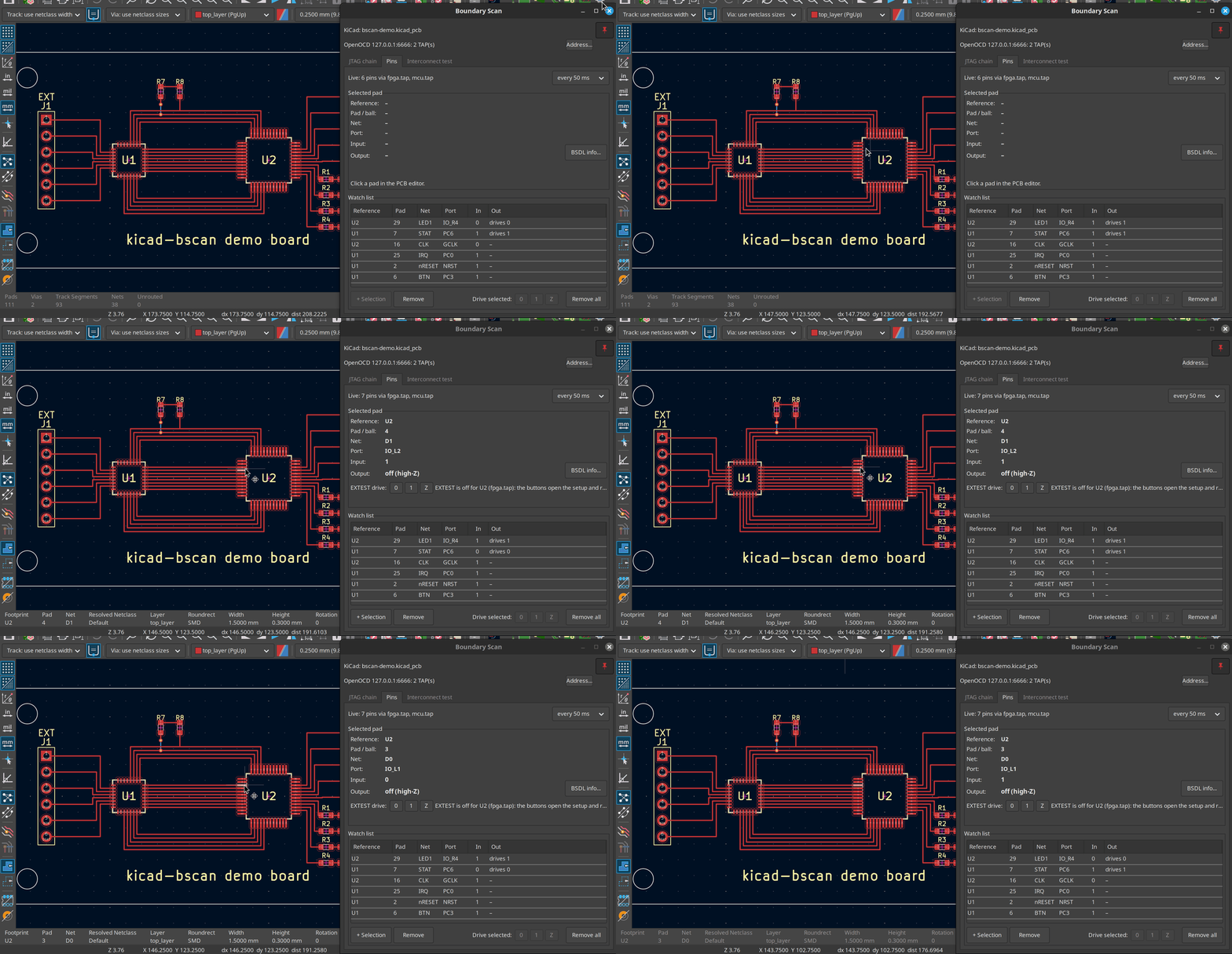
The demo board, simulated: pads clicked in the PCB editor, live values in the Pins tab.
Settings are stored per project in <project>.bscan.json next to the KiCad
project. Without a KiCad project (no board open, or no KiCad at all) they go
to a file of their own: by default no-project.bscan.json in the user's
configuration folder (~/.config/kicad-bscan/ on Linux, %APPDATA%\kicad-bscan\
on Windows); Settings file... opens another one or saves them as a new
one, e.g. one per board.
localhost:6666).The plugin is built from source.
1. Dependencies (Fedora):
sudo dnf install cmake gcc-c++ protobuf-devel protobuf-compiler nng-devel wxGTK-devel json-develNeeded: a C++23 compiler (GCC ≥ 13), wxWidgets ≥ 3.2, Protobuf, NNG, nlohmann/json ≥ 3.2.
Windows: built with MSYS2 in its UCRT64 environment (start the "MSYS2 UCRT64" shell):
pacman -S git mingw-w64-ucrt-x86_64-gcc mingw-w64-ucrt-x86_64-cmake \
          mingw-w64-ucrt-x86_64-ninja mingw-w64-ucrt-x86_64-protobuf \
          mingw-w64-ucrt-x86_64-nng mingw-w64-ucrt-x86_64-wxwidgets3.2-msw \
          mingw-w64-ucrt-x86_64-nlohmann-json
The steps below are the same in that shell. MSYS2 also has OpenOCD
(mingw-w64-ucrt-x86_64-openocd, without the optional extensions).
2. Source: libbsdl is a git submodule. Clone with --recursive, or
fetch it in an existing clone (also after a pull that moved it):
git submodule update --init3. Build and install:
cmake -S . -B build
cmake --build build -j
cmake --install build
This installs the plugin into the per-user plugin folder of your KiCad
version, e.g. ~/.local/share/kicad/9.0/plugins/ (Linux) or
Documents\KiCad\10.0\plugins\ (Windows) – the version is taken from
kicad-cli version; the configure step prints the folder it uses. To choose
it yourself: -DKICAD_VERSION=10.0 or -DKICAD_PLUGIN_DIR=/path/to/plugins.
(An existing build folder remembers the folder from its first configure; use
a fresh build folder or add -U KICAD_PLUGIN_DIR.)
On Windows the install also copies the DLLs the plugin needs (wxWidgets,
Protobuf, NNG, ...) next to kicad-bscan.exe; this needs CMake 3.21 or newer.
If a DLL is not found, the install stops and names it.
On Linux the install also adds a hidden kicad-bscan.desktop file and the
window icon to ~/.local/share – some desktops (GNOME on Wayland in
particular) take the taskbar icon only from there. Not wanted:
-DBSCAN_INSTALL_DESKTOP_FILE=OFF.
4. In KiCad:
demo/ has a small KiCad board with two simulated boundary-scan chips (a microcontroller and an FPGA) and a JTAG simulator for OpenOCD: pins, EXTEST and the interconnect test work as with a real board.
Start OpenOCD with your usual configuration, e.g.
openocd -f interface/... -f board/.... The plugin uses OpenOCD's Tcl
port, which is on by default (port 6666). If your configuration contains
tcl_port disabled, remove that line; if it uses another port, set it in
the plugin with Address....
Open the board in the PCB editor and click Boundary Scan. The window stays open while you work; pin (top right) keeps it on top. The window has three tabs: JTAG chain (setup), Pins (live values) and Interconnect test; the connection lines and the red EXTEST bar above them are always visible.
JTAG chain tab: the table lists the TAPs OpenOCD found. For each chip you want to use:
U1), or select the
footprint in KiCad and click ←.Settings of a TAP that is no longer in OpenOCD's chain stay in the table (grey, "not in chain"), e.g. while OpenOCD runs with another configuration; Forget... in that row removes them.
Pins tab: click a pad of that footprint in KiCad. Selected pad shows its net, the chip port, and the live input and output values.
Watch list: select pads in KiCad and click + Selection to keep them on the list.
One pin is selected everywhere: selecting rows in the watch list selects their pads in KiCad and highlights the pin in the chip view; selecting a pad in KiCad (or a pin in the chip view) selects its row in the watch list, if it is on the list.
The line at the top of the Pins tab shows what is being sampled and lets you set the sampling interval. The values are for looking at, not for timing measurements: depending on the adapter, a few to a few tens of samples per second are possible.
Chip view... (top right) opens a separate window that draws one chip of the chain with the live state of all its pins: drives 1 / 0, reads 1 / 0 (output off), toggling (drawn half 1, half 0), not sampled; JTAG, power and pins without boundary-scan cells in their own colours (legend below the drawing). Choose the chip at the top; it needs a BSDL file and a reference (JTAG chain tab).
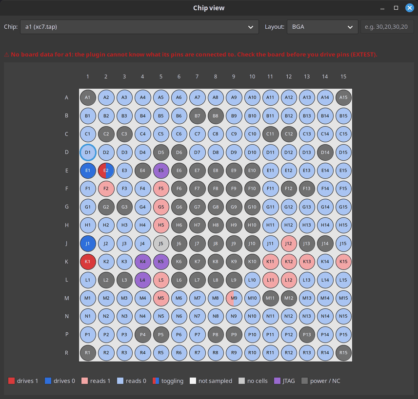
30,20,30,20 for left, bottom, right, top) or
dual (SOIC, TSSOP). It is saved per chip.Without KiCad: start the plugin directly – it is an ordinary program in
the plugin folder the install step printed, e.g.
~/.local/share/kicad/9.0/plugins/com.github.danselmi.kicad-bscan/kicad-bscan
(Linux) or Documents\KiCad\10.0\plugins\com.github.danselmi.kicad-bscan\kicad-bscan.exe
(Windows). The KiCad line then says "not connected"; the JTAG chain tab, the
Pins tab and the chip view work as usual (a reference is still needed per
chip: any name), and the settings go to a file of their own (see above).
BSDL folders... (JTAG chain tab, below the table) sets where to look; subfolders
are included (*.bsd, *.bsdl, *.bsm):
For a chip without a (matching) BSDL file, the plugin offers the files whose IDCODE and IR length match – one entry per file and package, best fitting first ("Pads found": how many of the footprint's pads exist in the package). Nothing is assigned automatically; you always choose.
The first search through a large collection takes a while (e.g. 20 s); afterwards results come from a cache and files are only read again when they change. Choosing the same BSDL file again re-reads it – handy when your FPGA tool regenerated it.
Warning. In EXTEST the boundary-scan register drives all pins of the chip, and the chip's own logic is disconnected from them. A wrong level can damage your hardware – think of a pin that drives a power stage, a bridge or an LED that is only meant to be pulsed. An FPGA may also lose its clock. Use EXTEST for bring-up and test preparation, not on a board doing its job.
Starting EXTEST – click EXTEST... in the chip's row, or one of the 0 / 1 / Z buttons of a pin (selected pad or watch list):
While EXTEST is active a red bar at the top says so and offers Leave EXTEST. Drive pins with the 0 / 1 / Z buttons of the selected pad, or Drive selected (or right-click) in the watch list; driven pins are marked with ▶. Changing a pin that shares its output enable with others asks first.
Safety rules built in:
jtag cur_ir, see below) to continue driving the same
states – or a new plan – without the pins returning to the chip's logic in
between. Several chips kept in EXTEST are taken over together (needs
jtag scan as well); you choose the states for each in turn.Keep OpenOCD quiet while in EXTEST. Anything else using the JTAG chain
can interrupt EXTEST: OpenOCD's background polling of targets in the same chain
(poll off stops it), or an IPDBG server. Each interruption hands the pins
back to the chip's logic for a moment.
jtag cur_ir (see below), interruptions are
detected: EXTEST and your pin states are restored at once, and the red bar
keeps a warning with the count and time of the last one. A board reset that
OpenOCD does not see (e.g. a reset button) is not detected, but the next
scan restores EXTEST all the same.The Interconnect test tab checks the soldering between the chips with BSDL files: every net that connects at least two of their boundary-scan pins is driven by one pin with a sequence of test patterns while the other pins listen. A net that reads another net's values is shorted to it; a pin that does not see its net is open.
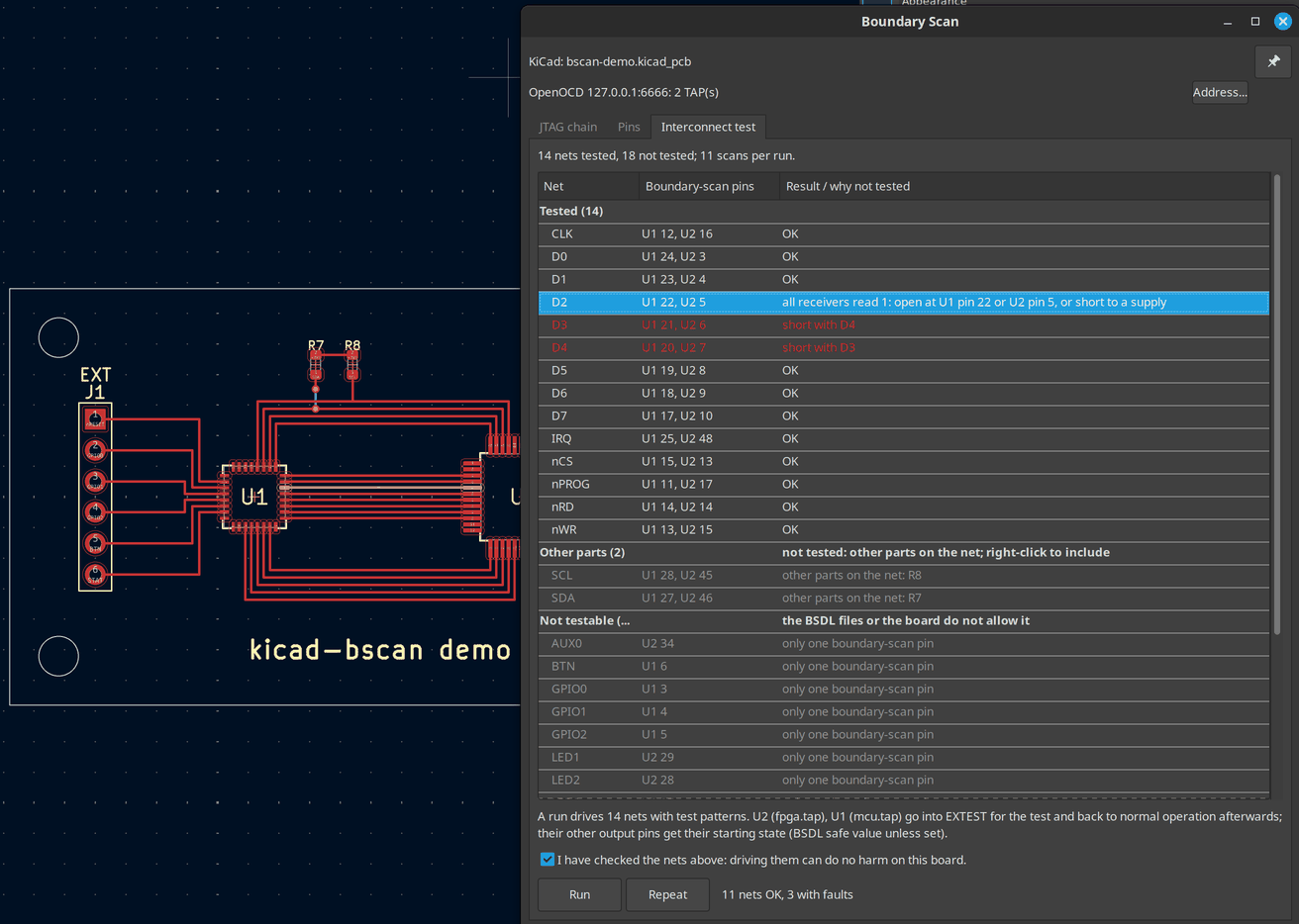
The demo board with a simulated short (D3–D4) and an open (U2 pin 5): the selected net D2 is highlighted in the PCB editor.
A test that involves several chips needs an OpenOCD with jtag scan (see
below); with a standard OpenOCD it runs only if all tested nets connect
pins of one chip.
The plugin works with a standard OpenOCD. Two additions make it better and are used automatically when available (not yet in upstream OpenOCD):
jtag cur_ir <tap> (change 9947) –
the instruction OpenOCD last loaded into a TAP. With it, the plugin knows
whether a chip is really in EXTEST (instead of "probably"), notices EXTEST
set by other programs, offers Take over, and detects interruptions of
EXTEST.jtag scan (change 9948) –
instruction and data scan as one operation, so nothing else (target
polling, IPDBG) can change the instruction in between. It scans several
chips at once, so with it several chips can be in EXTEST at the same
time (e.g. to test the connections between them), and the other chips keep
being sampled meanwhile.Both are in review for upstream OpenOCD. To use them now, build OpenOCD with
the two changes applied (each change page offers its patch under
Download). Whether your OpenOCD has them: help jtag in OpenOCD's console
(telnet port 4444) lists them.
9.0 or 10.0, see the configure output). KiCad skips
plugins it cannot load without a message; start it with
KICAD_ENABLE_WXTRACE=1 WXTRACE=KICAD_API kicad to see why.tcl_port disabled in the configuration), or it listens on
another address or port – use Address....jtag scan (see above) only one chip at a time can be in EXTEST,
and while it is, the other chips in the chain are not sampled (their pins
show "paused"): OpenOCD puts all other chips into BYPASS for every scan,
which would end EXTEST.GDK_BACKEND=x11 helps.GPL-3.0-only, see LICENSE. Included third-party code keeps its
license: libbsdl (MPL-2.0, submodule third_party/libbsdl/) and the KiCad API .proto
files (GPL-3.0-or-later, third_party/kicad-api/).
Problems, questions and ideas: please open an issue in this repository's issue tracker; pull requests are even better. Ideas already collected are in doc/TODO.md ("Ideas").
Build options, tests without hardware (JTAG simulator, fake KiCad server) and design notes: doc/DEVELOPMENT.md. Open points: doc/TODO.md.
| Qty | Value | Footprint | References |
|---|---|---|---|
| 4 | 330 | kicad-bscan-demo:R_0603_1608Metric | R1, R2, R3, R4 |
| 4 | LED | kicad-bscan-demo:LED_0603_1608Metric | D1, D2, D3, D4 |
| 2 | 4k7 | kicad-bscan-demo:R_0603_1608Metric | R7, R8 |
| 1 | BSDEMO_F48 | kicad-bscan-demo:TQFP-48_7x7mm_P0.5mm | U2 |
| 1 | BSDEMO_M32 | kicad-bscan-demo:QFN-32_5x5mm_P0.5mm | U1 |
| 1 | EXT | kicad-bscan-demo:PinHeader_1x06_P2.54mm | J1 |
| 1 | SPI | kicad-bscan-demo:PinHeader_1x05_P2.54mm | J2 |
It measures 68 × 34 mm and has 2 copper layers, 1.6 mm thick.
14 parts. The full list of its parts is on this page, with links to each part's symbol and footprint where PCBKit's library has them.
From the danselmi/kicad-bscan repository on GitHub, at the commit this page was made from: the board is demo/bscan-demo/bscan-demo.kicad_pcb. PCBKit opens the board in the browser, with nothing to install.
Its repository publishes it under the GPL-3.0 licence: you may reuse it on that licence's terms (keep the author's notice, and for a copyleft licence share your changes alike).
google/mozc-devices
Circuit diagrams and firmware source code for Gboard DIY keyboards


hackclub/OnBoard
💡 Join 1,000 teenagers and make your first PCB with a $100 grant!


Twotoz/C5VRX
Ultra-minimal, zero-CPU 5.8 GHz analog FPV video receiver using ESP32-C5 Wi-Fi 6 PHY MODEM_DIAG, BitScrambler WBFM demodulation & resistor DAC CVBS

