
2 layers210.1 × 69.6 mm
 Danmuse/Lab_EA1_FRBA2
This project covers the design and verification of single-stage amplifier circuits using bipolar and field-effect transistors.
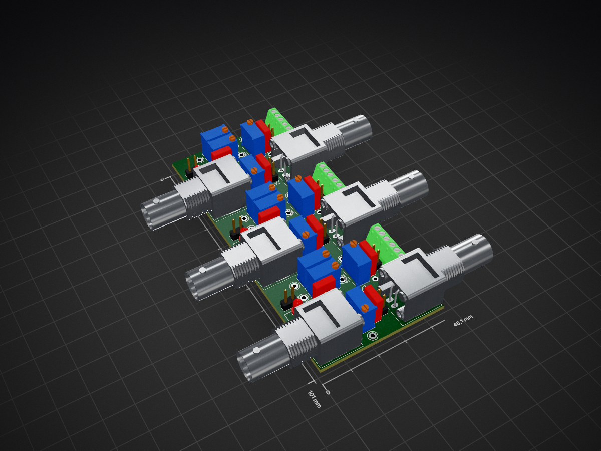
LabEA1 is an open-source printed circuit board by Danmuse, from the Danmuse/Lab_EA1_FRBA repository on GitHub. It is a 2-layer board of 45.1 × 101 mm with 81 parts on 22 nets, routed with 773 tracks and 0 vias.
It is built around the SMAJ12A. Its parts include 39 connectors, 9 capacitors and 3 diodes. It belongs with the audio and music boards of this library.
The Single-stage amplifiers project involves the design, simulation, and experimental validation of single-stage amplifier circuits using bipolar junction transistors (BJTs) and field-effect transistors (FETs). The main objective is to compare theoretical small-signal and biasing calculations with actual laboratory measurements.
20 MH16 MH0 MH0 MH0 MH0 MH[!TIP] This section showcases the transition from theoretical design to physical implementation.
| Schematic circuit | PCB (TOP view) | PCB (BOTTOM view) + Layout |
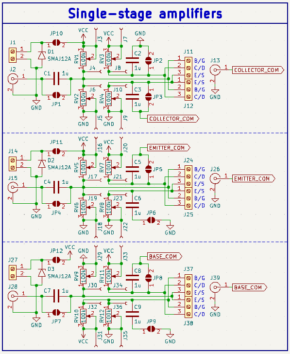 | 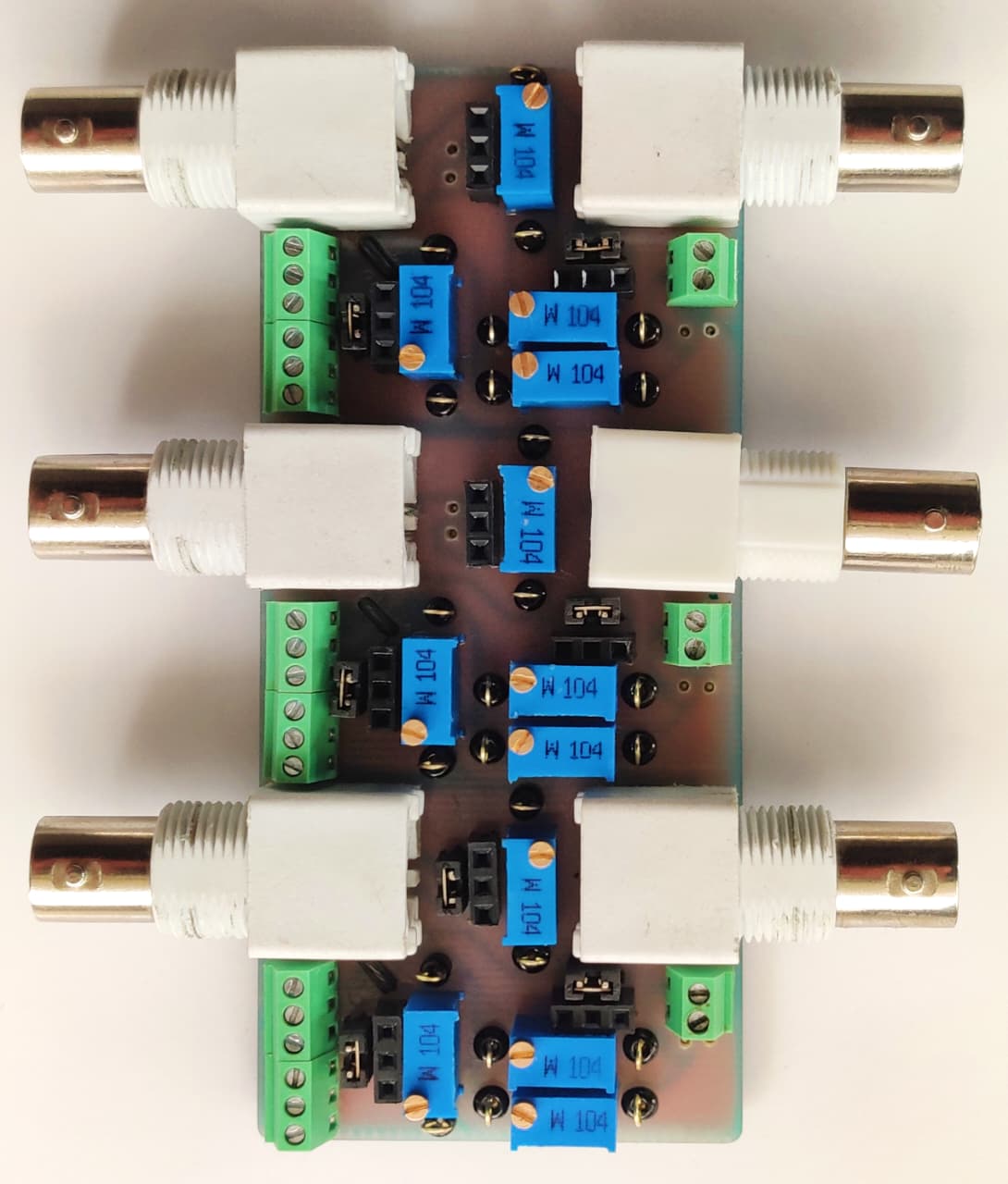 | 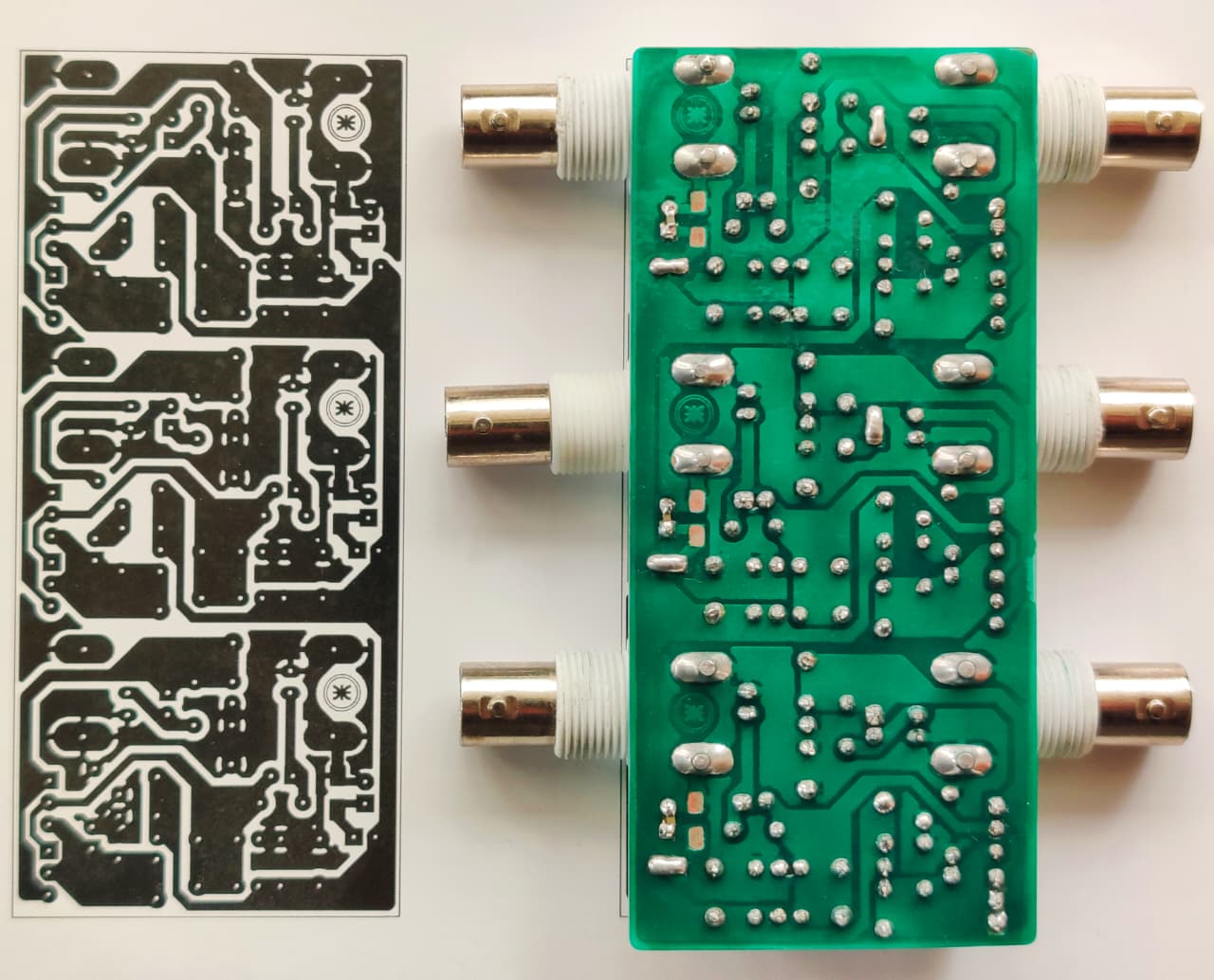 |
| Qty | Value | Footprint | References |
|---|---|---|---|
| 24 | Conn_01x01_Socket | 5006:5006 | J3, J10, J16, J17, J18, J19, J20, J21, J22, J23, J29, J30, J31, J32, J33, J34 +8 |
| 12 | 100k | Potentiometer_THT:Potentiometer_Bourns_3296W_Vertical | RV1, RV2, RV3, RV4, RV5, RV6, RV7, RV8, RV9, RV10, RV11, RV12 |
| 12 | SolderJumper_2_Open | Connector_PinHeader_2.54mm:PinHeader_1x02_P2.54mm_Vertical | JP1, JP2, JP3, JP4, JP5, JP6, JP7, JP8, JP9, JP10, JP11, JP12 |
| 9 | 1u | Capacitor_THT:C_Rect_L7.0mm_W2.5mm_P5.00mm | C1, C2, C3, C4, C5, C6, C7, C8, C9 |
| 6 | , , , , , | ||
| 6 | Conn_Coaxial | Connector_Coaxial:BNC_Amphenol_B6252HB-NPP3G-50_Horizontal | J2, J13, J15, J26, J28, J39 |
| 6 | Screw_Terminal_01x03 | TBC05_03_0_1_G_G:1725669 | J11, J12, J24, J25, J37, J38 |
| 3 | SMAJ12A | Diode_SMD:D_SMA | D1, D2, D3 |
| 3 | Screw_Terminal_01x02 | TBC05_02_0_1_G_G:1725656 | J1, J14, J27 |

Jeo0/atg-client
automatic trajectory generator cross-platform client for acoustic volumetric displays (dis our thesis :))

dxy250312/-RK3588-PCB-YOLO-
基于 YOLOv11 与 ELF 2(RK3588)的 PCB 裸板缺陷检测系统。项目包含模型训练、数据集配置、RKNN 部署、Qt 可视化界面以及 RK3588 GPIO 控制示例,可用于学习边缘 AI 在工业视觉中的应用。

kuellenberg/Dew-Controller
Dew heater controller for telescope dew heater straps

yousseftamer-eng/Ratatouille_3_Micromouse
Remi 3 — micromouse robot that won 2nd place at IEEE Mansoura's Victories 4 micromouse competition. Includes PCB schematics, fabrication files, CAD models, and firmware.


HeyPCB/knuckle
35 mm round FOC driver for a GBM2804 gimbal motor that answers on the Open Duck Mini's servo bus as an STS3215. 6-layer KiCad 10 board plus printed standoff, cover and horn adapter.

It measures 45.1 × 101 mm and has 2 copper layers, 1.6 mm thick.
81 parts, built around the SMAJ12A. The full list of its parts is on this page, with links to each part's symbol and footprint where PCBKit's library has them.
From the Danmuse/Lab_EA1_FRBA repository on GitHub, at the commit this page was made from: the board is PCB Design/LabEA1/LabEA1.kicad_pcb and its schematic PCB Design/LabEA1/LabEA1.kicad_sch. PCBKit opens the board in the browser, with nothing to install.
Its repository states no licence, so its author keeps all rights: ask Danmuse before reusing the design.