

4 layers40 × 25 mm
 danislab/MicroLabBox-LaunchPad-Interface
A Interface PCB to connect LaunchPads from TI to the MicroLabBox from dSPACE to perform Hardware-in-the-Loop validation tests
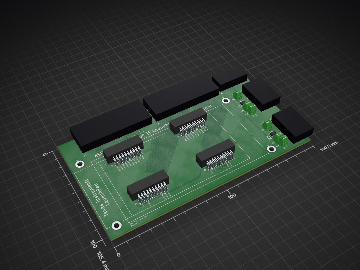
LaunchPad MLB Adapter is an open-source printed circuit board by danislab, from the danislab/MicroLabBox-LaunchPad-Interface repository on GitHub. It is a 2-layer board of 190.5 × 105.4 mm with 29 parts on 133 nets, routed with 459 tracks and 30 vias.
It is built around the SN65HVD234DR-JSM and RC0402FR-0710KL. Its parts include 15 connectors, 6 resistors, 2 capacitors and 2 ICs. It belongs with the interfaces and adapters boards of this library.
The MicroLabBox LaunchPad Interface is a simple PCB to connect LaunchPads from Texas Instruments (TI) to the MicroLabBox from dSPACE to perform real-time Hardware-in-the-Loop (HIL) tests. This Interface PCB can be used to accelerate the development and validation of software and algorithms running on MCUs from TI. Depending on the LaunchPad the interface PCB offers up to 28 digital IOs, 16 analog inputs (LaunchPad side), 4 analog outputs (LaunchPad side) and two independent CAN interfaces.
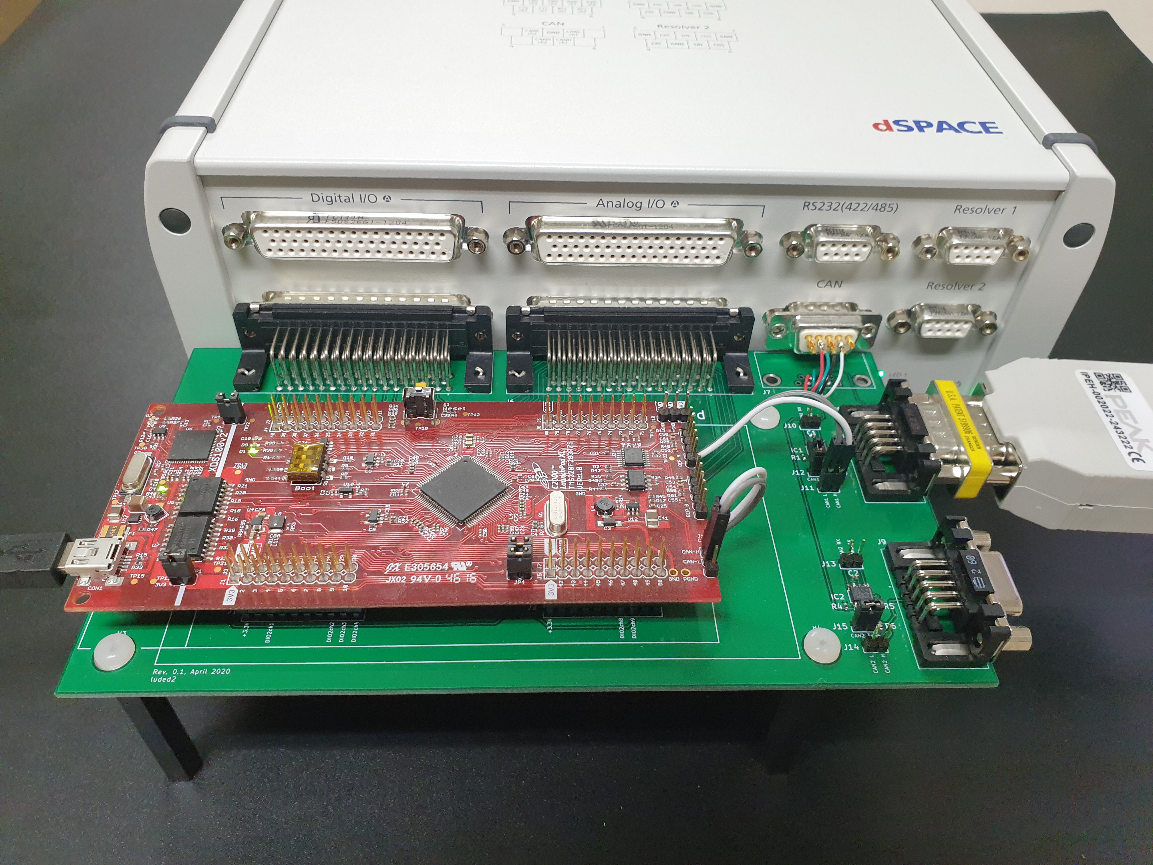
The pinout of the CAN interface follows the ISO 11898 specification
The pinout of the connectors J1 - J4 is described in the following table.
| TIBoosterPack standard | F28377S | F28379D | TMS 570LS12x and TMS 570LC43x | dSPace MicroLabBox | |||
|---|---|---|---|---|---|---|---|
| Connector | Pin | Function | Function | Function | Connector | Pin | Function |
| J1 | 1 | +3.3 V | +3.3V | +3.3 V | |||
| J1 | 2 | GPIO71 | GPIO32 | AD1IN[16] | |||
| J1 | 3 | GPIO90 | GPIO19 | SCIRX | |||
| J1 | 4 | GPIO89 | GPIO18 | SCITX | |||
| J1 | 5 | GPIO41 | GPIO67 | GIOA[7] | Digital I/O B | 33 | DIO2ch1 |
| J1 | 6 | NC | GPIO111 | AD1IN[17] | |||
| J1 | 7 | GPIO60 | GPIO60 | MIBSPI3CLK | |||
| J1 | 8 | GPIO61 | GPIO22 | GIOA[6] | Digital I/O B | 32 | DIO2ch2 |
| J1 | 9 | GPIO43 | GPIO105 | N2HET1[4] | Digital I/O B | 31 | DIO2ch3 |
| J1 | 10 | GPIO42 | GPIO104 | N2HET1[9] | Digital I/O B | 29 | DIO2ch4 |
| J2 | 20 | GND | GND | GND | |||
| J2 | 19 | GPIO4 | GPIO61 | N2HET1[22] | |||
| J2 | 18 | GPIO62 | GPIO123 | MIBSPI3NCS[1] | |||
| J2 | 17 | NC | GPIO122 | GIOB[3] | |||
| J2 | 16 | RESET | RESET | RESET | |||
| J2 | 15 | GPIO58 | GPIO58 | MIBSPI3SIMO | |||
| J2 | 14 | GPIO59 | GPIO59 | MIBSPI3SOMI | |||
| J2 | 13 | GPIO72 | GPIO124 | N2HET1[27] | Digital I/O B | 28 | DIO2ch5 |
| J2 | 12 | GPIO73 | GPIO125 | N2HET1[29] | Digital I/O B | 27 | DIO2ch6 |
| J2 | 11 | GPIO78 | GPIO29 | GIOB[2] | Digital I/O B | 25 | DIO2ch7 |
| J3 | 21 | +5 V | +5 V | +5 V | |||
| J3 | 22 | GND | GND | GND | |||
| J3 | 23 | ADCIN14 | ADCIN14 | AD1[0] | Analog I/O B | 49 | AO1ch1 |
| J3 | 24 | ADCINB1 | ADCINC3 | AD1[7] | Analog I/O B | 32 | AO1ch2 |
| J3 | 25 | ADCINB4 | ADCINB3 | AD1IN[18] | Analog I/O B | 47 | AO1ch3 |
| J3 | 26 | ADCINB2 | ADCINA3 | AD1IN[19] | Analog I/O B | 30 | AO1ch4 |
| J3 | 27 | ADCINA0 | ADCINC2 | AD1IN[20] | Analog I/O B | 45 | AO1ch5 |
| J3 | 28 | ADCINB0 | ADCINB2 | AD1IN[21] | Analog I/O B | 28 | AO1ch6 |
| J3 | 29 | ADCINA1 | ADCINA2 | Analog I/O B | 43 | AO1ch7 | |
| J3 | 30 | NC | ADCINA0 | Analog I/O B | 26 | AO1ch8 | |
| J4 | 40 | GPIO12 | GPIO0 | N2HET1[20] | Digital I/O B | 17 | DIO1ch33 |
| J4 | 39 | GPIO13 | GPIO1 | N2HET1[18] | Digital I/O B | 16 | DIO1ch34 |
| J4 | 38 | GPIO14 | GPIO2 | N2HET1[16] | Digital I/O B | 15 | DIO1ch35 |
| J4 | 37 | GPIO15 | GPIO3 | N2HET1[30] | Digital I/O B | 14 | DIO1ch36 |
| J4 | 36 | GPIO16 | GPIO4 | N2HET1[14] | Digital I/O B | 13 | DIO1ch37 |
| J4 | 35 | GPIO17 | GPIO5 | N2HET1[12] | Digital I/O B | 12 | DIO1ch38 |
| J4 | 34 | GPIO20 | GPIO24 | GIOA[5] | Digital I/O B | 11 | DIO1ch39 |
| J4 | 33 | GPIO21 | GPIO16 | GIOA[2] | Digital I/O B | 10 | DIO1ch40 |
| J4 | 32 | DAC1 | DAC1 | GIOA[1] | Analog I/O B | 17 | AI2ch1 |
| J4 | 31 | DAC2 | DAC2 | GIOA[0] | Analog I/O B | 15 | AI2ch2 |
| J6 | 41 | +3.3 V | +3.3 V | +3.3 V | |||
| J6 | 42 | NC | GPIO95 | AD1IN[9] | |||
| J6 | 43 | GPIO87 | GPIO139 | LIN1_RXD | |||
| J6 | 44 | GPIO86 | GPIO56 | LIN1_TXD | |||
| J6 | 45 | NC | GPIO97 | GIOB[2] | |||
| J6 | 46 | NC | GPIO94 | AD1IN[1] | |||
| J6 | 47 | GPIO65 | GPIO65 | MIBSPI1CLK | Digital I/O B | 24 | DIO2ch8 |
| J6 | 48 | NC | GPIO52 | N2HET1[31] | Digital I/O B | 23 | DIO2ch9 |
| J6 | 49 | GPIO69 | GPIO41 | N2HET1[24] | |||
| J6 | 50 | GPIO66 | GPIO40 | N2HET1[26] | |||
| J7 | 60 | GND | GND | GND | |||
| J7 | 59 | GPIO91 | GPIO66 | N2HET2[8] | |||
| J7 | 58 | NC | GPIO131 | MIBSPI1SOMI[1] | |||
| J7 | 57 | NC | GPIO130 | MIBSPI5SIMO[0] | |||
| J7 | 56 | RESET | RESET | RESET | |||
| J7 | 55 | GPIO63 | GPIO63 | MIBSPI1SIMO | |||
| J7 | 54 | GPIO64 | GPIO64 | MIBSPI1SOMI | |||
| J7 | 53 | GPIO99 | GPIO26 | N2HET1[17] | Digital I/O B | 21 | DIO2ch10 |
| J7 | 52 | GPIO92 | GPIO27 | N2HET1[19] | Digital I/O B | 20 | DIO2ch11 |
| J7 | 51 | NC | GPIO25 | MIBSPI5SOMI[0] | Digital I/O B | 19 | DIO2ch12 |
| J8 | 61 | +5 V | +5 V | +5 V | |||
| J8 | 62 | GND | GND | GND | |||
| J8 | 63 | ADCIN15 | ADCIN15 | AD1IN[10] | Analog I/O B | 41 | AO1ch9 |
| J8 | 64 | ADCINA2 | ADCINC5 | AD1IN[2] | Analog I/O B | 24 | AO1ch10 |
| J8 | 65 | ADCINA5 | ADCINB5 | AD1IN[3] | Analog I/O B | 39 | AO1ch11 |
| J8 | 66 | ADCINB5 | ADCINA5 | AD1IN[11] | Analog I/O B | 22 | AO1ch12 |
| J8 | 67 | ADCINA3 | ADCINC4 | AD1IN[4] | Analog I/O B | 37 | AO1ch13 |
| J8 | 68 | ADCINB3 | ADCINB4 | AD1IN[12] | Analog I/O B | 20 | AO1ch14 |
| J8 | 69 | ADCINA4 | ADCINA4 | NC | Analog I/O B | 35 | AO1ch15 |
| J8 | 70 | NC | ADCINA1 | NC | Analog I/O B | 18 | AO1ch16 |
| J9 | 80 | GPIO2 | GPIO6 | N2HET1[10] | Digital I/O B | 9 | DIO1ch41 |
| J9 | 79 | GPIO3 | GPIO7 | N2HET1[28] | Digital I/O B | 8 | DIO1ch42 |
| J9 | 78 | GPIO10 | GPIO8 | N2HET1[8] | Digital I/O B | 7 | DIO1ch43 |
| J9 | 77 | GPIO11 | GPIO9 | N2HET1[23] | Digital I/O B | 6 | DIO1ch44 |
| J9 | 76 | GPIO18 | GPIO10 | MIBSPI5NENA | Digital I/O B | 5 | DIO1ch45 |
| J9 | 75 | GPIO19 | GPIO11 | N2HET2[18] | Digital I/O B | 4 | DIO1ch46 |
| J9 | 74 | NC | GPIO14 | GIOB[1] | Digital I/O B | 3 | DIO1ch47 |
| J9 | 73 | NC | GPIO15 | GIOB[0] | Digital I/O B | 2 | DIO1ch48 |
| J9 | 72 | DAC3 | DAC3 | AD1EVT | Analog I/O B | 13 | AI2ch3 |
| J9 | 71 | DAC4 | DAC4 | MIBSPI5CLK | Analog I/O B | 11 | AI2ch4 |
| Qty | Value | Footprint | References |
|---|---|---|---|
| 6 | 61300211121 | SamacSys_Parts:HDRV2W110P0X254_1X2_508X254X854P | J10, J11, J12, J13, J14, J15 |
| 4 | 61302021121 | SamacSys_Parts:HDRV20W64P254X254_2X10_2540X508X869P | J1, J2, J3, J4 |
| 4 | MountingHole_Pad | MountingHole:MountingHole_4.3mm_M4_DIN965_Pad | H1, H2, H3, H4 |
| 4 | RC0402FR-0710KL | SamacSys_Parts:RESC1005X40N | R1, R2, R4, R5 |
| 2 | 09661526613 | SamacSys_Parts:09661526613 | J8, J9 |
| 2 | 09665627812 | SamacSys_Parts:09665627812 | J5, J6 |
| 2 | GRM155R61A104KA01D | SamacSys_Parts:CAPC1005X55N | C1, C2 |
| 2 | RC0603FR-07120RL | SamacSys_Parts:RESC1608X55N | R3, R6 |
| 2 | SN65HVD234DR | SamacSys_Parts:SOIC127P600X175-8N | IC1, IC2 |
| 1 | 09661626812 | SamacSys_Parts:09661626812 | J7 |
It measures 190.5 × 105.4 mm and has 2 copper layers, 1.6 mm thick.
29 parts, built around the SN65HVD234DR-JSM and RC0402FR-0710KL. The full list of its parts is on this page, with links to each part's symbol and footprint where PCBKit's library has them.
From the danislab/MicroLabBox-LaunchPad-Interface repository on GitHub, at the commit this page was made from: the board is LaunchPad_MLB_Adapter.kicad_pcb. PCBKit opens the board in the browser, with nothing to install.
Its repository states no licence, so its author keeps all rights: ask danislab before reusing the design.


MiniNugen/Custom_Inverter_Hardware
PCBProjectNameREV1.PrjPCB | Source Documents | | PCBProjectNameREV1.SchDOC | | PCBProjectNameREV1.PcbDOC | | BOM | Settings | Libraries


