
2 layers35 × 25 mm
Task1
dae9999nam/SL_Blog
This repository is to record comprehensive learning of technology and package from ELEC2840
5 parts
 dae9999nam/SL_Blog
This repository is to record comprehensive learning of technology and package from ELEC2840
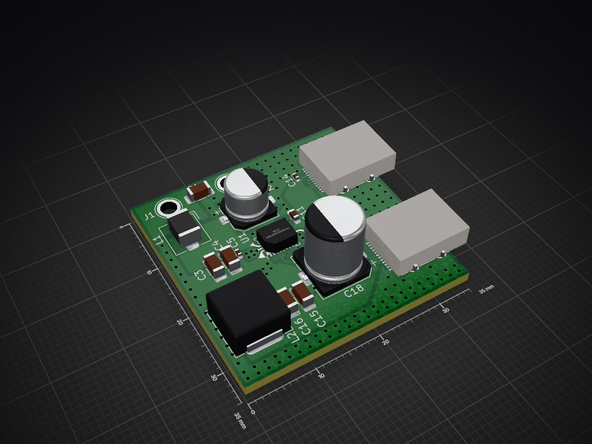
Task4 is an open-source printed circuit board by dae9999nam, from the dae9999nam/SL_Blog repository on GitHub. It is a 4-layer board of 35 × 35 mm with 36 parts on 43 nets, routed with 219 tracks and 243 vias.
It is built around the TPS25858QRPQRQ1. Its parts include 18 capacitors, 10 resistors, 4 connectors, 2 inductors and 1 IC. It belongs with the home automation and IoT boards of this library.
| Qty | Value | Footprint | References |
|---|---|---|---|
| 5 | 0U1/50V | Tutorial2:C_0402_1005Metric_Pad0.74x0.62mm_HandSolder | C5, C8, C13, C14, C17 |
| 3 | 0 | Tutorial2:R_0402_1005Metric_Pad0.72x0.64mm_HandSolder | R3, R4, R8 |
| 3 | 10U/50V | Tutorial2:C_1206_3216Metric_Pad1.33x1.80mm_HandSolder | C1, C3, C4 |
| 3 | 22U/10V | Tutorial2:C_1206_3216Metric_Pad1.33x1.80mm_HandSolder | C12, C15, C16 |
| 2 | 1502-2 | Tutorial2:Terminal_Keystone_1502-2 | J1, J2 |
| 2 | 1U/16V | Tutorial2:C_0603_1608Metric_Pad1.08x0.95mm_HandSolder | C10, C11 |
| 2 | 20K | Tutorial2:R_0402_1005Metric_Pad0.72x0.64mm_HandSolder | R5, R6 |
| 2 | 2U2/10V | Tutorial2:C_0603_1608Metric_Pad1.08x0.95mm_HandSolder | C6, C9 |
| 2 | 5K1 | Tutorial2:R_0402_1005Metric_Pad0.72x0.64mm_HandSolder | R9, R10 |
| 2 | USB_C_Plug_632723300011 | Tutorial2:USB_C_Plug_632723300011 | J3, J4 |
| 1 | 0U1/16V | Tutorial2:C_0402_1005Metric_Pad0.74x0.62mm_HandSolder | C7 |
| 1 | 100U/50V | Tutorial2:CP_Elec_6.3x5.8 | C2 |
| 1 | 18K7/1% | Tutorial2:R_0402_1005Metric_Pad0.72x0.64mm_HandSolder | R2 |
| 1 | 330U/10V | Tutorial2:CP_Elec_8x10 | C18 |
| 1 | 39K2/1% | Tutorial2:R_0402_1005Metric_Pad0.72x0.64mm_HandSolder | R1 |
| 1 | 470K | Tutorial2:R_0402_1005Metric_Pad0.72x0.64mm_HandSolder | RT1 |
| 1 | 49K9/1% | Tutorial2:R_0402_1005Metric_Pad0.72x0.64mm_HandSolder | R7 |
| 1 | L-Panasonic-ETQP4M4R7KVK | Tutorial2:L_Panasonic_M0840 | L2 |
| 1 | L-Wurth-5030 | Tutorial2:L_Wurth_5030 | L1 |
| 1 | TPS25858QRPQRQ1 | Tutorial2:RPQ0025A | U1 |
dae9999nam/SL_Blog
This repository is to record comprehensive learning of technology and package from ELEC2840

joeycastillo/Sensor-Watch
A board replacement for the classic Casio F-91W wristwatch


rjwalters/kicad-tools
Standalone Python tools for parsing and manipulating KiCad schematic and PCB files

mbtaylor1982/ReSDMAC
Verilog code to replace the Commodore SDMAC found in the A3000


dmkfasi/nus-cpu
This tends to re-create Nintendo 64 schematics and lay out a board suitable for portable version
It measures 35 × 35 mm and has 4 copper layers, 1.6 mm thick.
36 parts, built around the TPS25858QRPQRQ1. The full list of its parts is on this page, with links to each part's symbol and footprint where PCBKit's library has them.
From the dae9999nam/SL_Blog repository on GitHub, at the commit this page was made from: the board is PCB/Day2/Task4.kicad_pcb. PCBKit opens the board in the browser, with nothing to install.
Its repository states no licence, so its author keeps all rights: ask dae9999nam before reusing the design.