4 layers223 × 50 mm
MainClockPCB
njKessel/ESP32s3-NetworkClock
ESP32-S3 smart clock with LED display, weather, moon phase, temperature, Google Calendar
69 parts1MIT

 d3vf1x/MSN
Wireless Enviromental Sensor that can make use of multiple IoT technologies.
MSN is an open-source printed circuit board by d3vf1x, from the d3vf1x/MSN repository on GitHub, published under the GPL-3.0 licence. It is a 2-layer board of 68 × 66 mm with 44 parts on 43 nets, routed with 419 tracks and 80 vias.
It is built around the ESP32-C6-WROOM-1-N4, BME680 and MAX16150AUT+T, with the PCF85363ATT/AJ and AB26T-32.768KHZ-6 among its other parts. Its parts include 11 resistors, 6 capacitors, 5 ICs, 2 connectors and 1 diode. It belongs with the home automation and IoT and sensors and measurement boards and the ESP32 and RISC-V boards of this library.


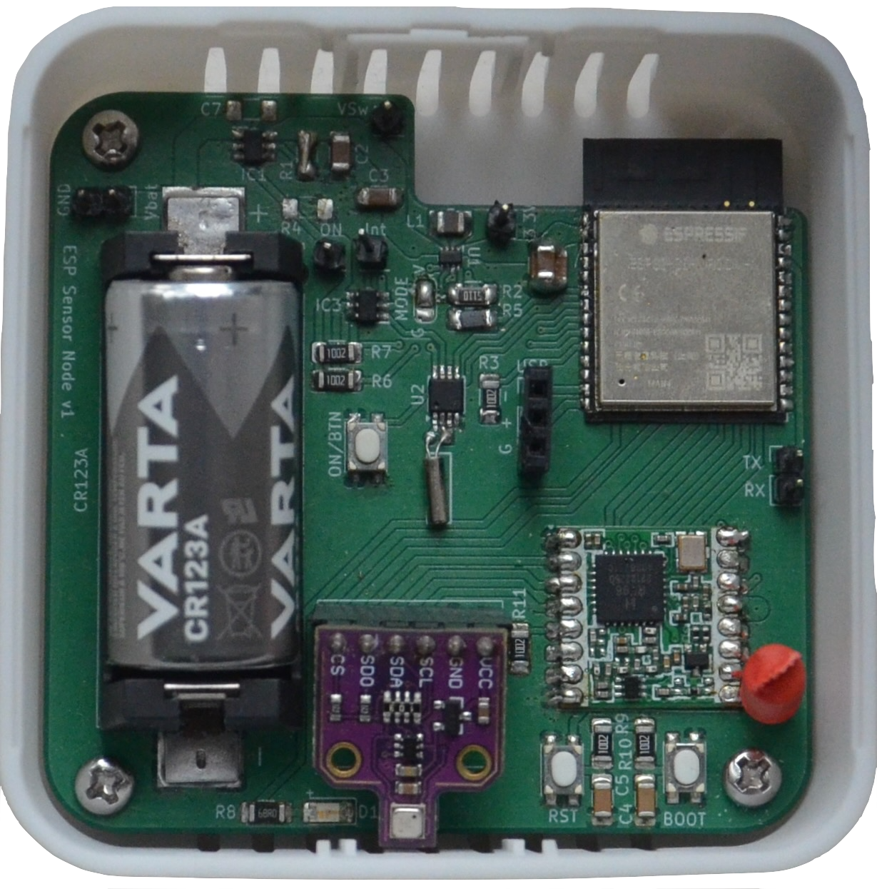
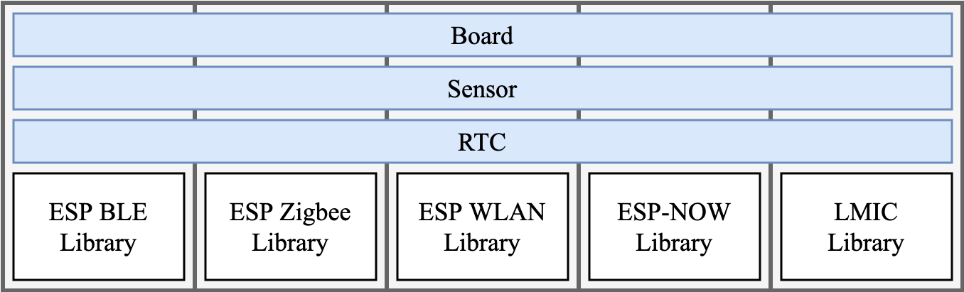
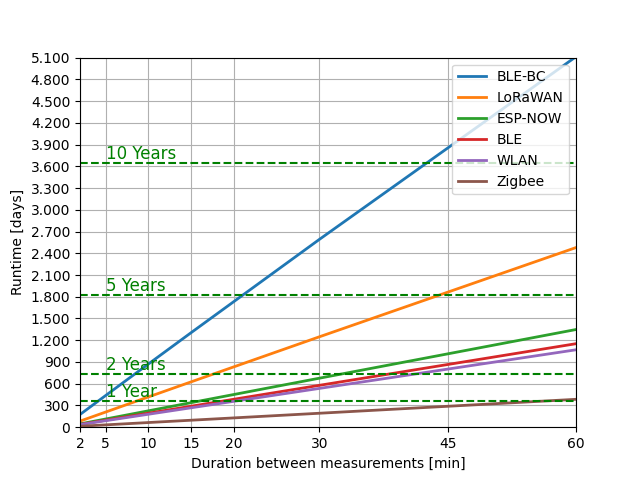
Wireless Enviromental Sensor that can make use of multiple IoT technologies.
| Qty | Value | Footprint | References |
|---|---|---|---|
| 4 | 10K | Resistor_SMD:R_1206_3216Metric_Pad1.30x1.75mm_HandSolder | R3, R9, R10, R11 |
| 3 | 10k | Resistor_SMD:R_1206_3216Metric_Pad1.30x1.75mm_HandSolder | R4, R6, R7 |
| 3 | MountingHole | MountingHole:MountingHole_3.2mm_M3 | H1, H2, H3 |
| 2 | 0.1uF | Capacitor_SMD:C_1206_3216Metric_Pad1.33x1.80mm_HandSolder | C4, C5 |
| 2 | 47uF | Capacitor_SMD:C_1206_3216Metric_Pad1.33x1.80mm_HandSolder | C1, C2 |
| 1 | 0 | Resistor_SMD:R_1206_3216Metric_Pad1.30x1.75mm_HandSolder | R1 |
| 1 | 1uH | Inductor_SMD:L_1008_2520Metric_Pad1.43x2.20mm_HandSolder | L1 |
| 1 | 22uF | Capacitor_SMD:C_1206_3216Metric_Pad1.33x1.80mm_HandSolder | C3 |
| 1 | 511 | Resistor_SMD:R_1206_3216Metric_Pad1.30x1.75mm_HandSolder | R5 |
| 1 | 68 | Resistor_SMD:R_1206_3216Metric_Pad1.30x1.75mm_HandSolder | R8 |
| 1 | 91 | Resistor_SMD:R_1206_3216Metric_Pad1.30x1.75mm_HandSolder | R2 |
| 1 | AB26T/32,768kHz | Crystal:Crystal_AB26T_Horizontal | Y1 |
| 1 | ANT | Connector_PinHeader_2.54mm:PinHeader_1x01_P2.54mm_Vertical | ANT |
| 1 | BME680 | Sensor:BME680_Board | J3 |
| 1 | Boot | Button_Switch_SMD:SW_Push_3x4x2.5 | BOOT |
| 1 | C | Capacitor_SMD:C_1206_3216Metric_Pad1.33x1.80mm_HandSolder | C7 |
| 1 | CR123a (BX0123) | Battery:BatteryHolder_Eagle_CR123A_12BH23PGR | BT1 |
| 1 | Debug 2.1V/20mA | LED_SMD:LED_1206_3216Metric_Pad1.42x1.75mm_HandSolder | D1 |
| 1 | ESP32-C6-WROOM-1-N4 | RF_Module:ESP32-C6-WROOM1-N4 | ESP32-C6 |
| 1 | INT | Connector_PinHeader_2.54mm:PinHeader_1x01_P2.54mm_Vertical | Int |
| 1 | LOGO | LOGO | G*** |
| 1 | MAX16150AUT+T | Package_SO:SOT95P280X145-6N | IC3 |
| 1 | Mode Select | Jumper:SolderJumper-3_P1.3mm_Bridged12_RoundedPad1.0x1.5mm_NumberLabels | JP1 |
| 1 | On/SW_2 | Button_Switch_SMD:SW_Push_3x4x2.5 | ON/BTN |
| 1 | Out | Connector_PinHeader_2.54mm:PinHeader_1x01_P2.54mm_Vertical | ON |
| 1 | PCF85363ATT/A | Package_SO:TSSOP-8_3x3mm_P0.65mm | U2 |
| 1 | RFM96W-315S2 | RF_Module:HOPERF_RFM9XW_SMD | U3 |
| 1 | RST | Button_Switch_SMD:SW_Push_3x4x2.5 | RST |
| 1 | TPS22917DBVT | Package_SO:SOT95P280X145-6N | IC1 |
| 1 | TPS631000DRLR | Package_SO:SOTFL50P160X60-8N | U1 |
| 1 | TX/RX | Connector_PinHeader_2.54mm:PinHeader_1x03_P2.54mm_Vertical | J3 |
| 1 | USB | Connector_PinHeader_2.54mm:PinHeader_1x03_P2.54mm_Vertical | JUSB |
| 1 | VBat | Connector_PinHeader_2.54mm:PinHeader_1x02_P2.54mm_Vertical | Vbat |
| 1 | VSw | Connector_PinHeader_2.54mm:PinHeader_1x01_P2.54mm_Vertical | VSw |
| 1 | Vout | Connector_PinHeader_2.54mm:PinHeader_1x01_P2.54mm_Vertical | 3.3V |
It measures 68 × 66 mm and has 2 copper layers, 1.6 mm thick.
44 parts, built around the ESP32-C6-WROOM-1-N4, BME680, MAX16150AUT+T and PCF85363ATT/AJ. The full list of its parts is on this page, with links to each part's symbol and footprint where PCBKit's library has them.
From the d3vf1x/MSN repository on GitHub, at the commit this page was made from: the board is pcb/MSN.kicad_pcb and its schematic pcb/MSN.kicad_sch. PCBKit opens the board in the browser, with nothing to install.
Its repository publishes it under the GPL-3.0 licence: you may reuse it on that licence's terms (keep the author's notice, and for a copyleft licence share your changes alike).
njKessel/ESP32s3-NetworkClock
ESP32-S3 smart clock with LED display, weather, moon phase, temperature, Google Calendar


punkfab/pcb-corpus
235 real KiCad boards from open-source hardware repositories, prepared as a placement and routing benchmark

antmicro/rdimm-ddr4-tester
Experimental platform built around Xilinx Kintex-7 FPGA for development and customization of RAM controllers supporting RDIMM DDR4 RAM modules used in data centers.


