
2 layers90 × 92 mm

 csu-grenoble/flatsat3
Extensions to flatsat mockup
Com Nucleo L432kc is an open-source printed circuit board by csu-grenoble, from the csu-grenoble/flatsat repository on GitHub. It is a 2-layer board of 90 × 92 mm with 47 parts on 99 nets, routed with 480 tracks and 92 vias.
It is built around the L9616 and MIKROE-4247. Its parts include 14 resistors, 10 capacitors, 7 connectors, 2 ICs and 1 switch.
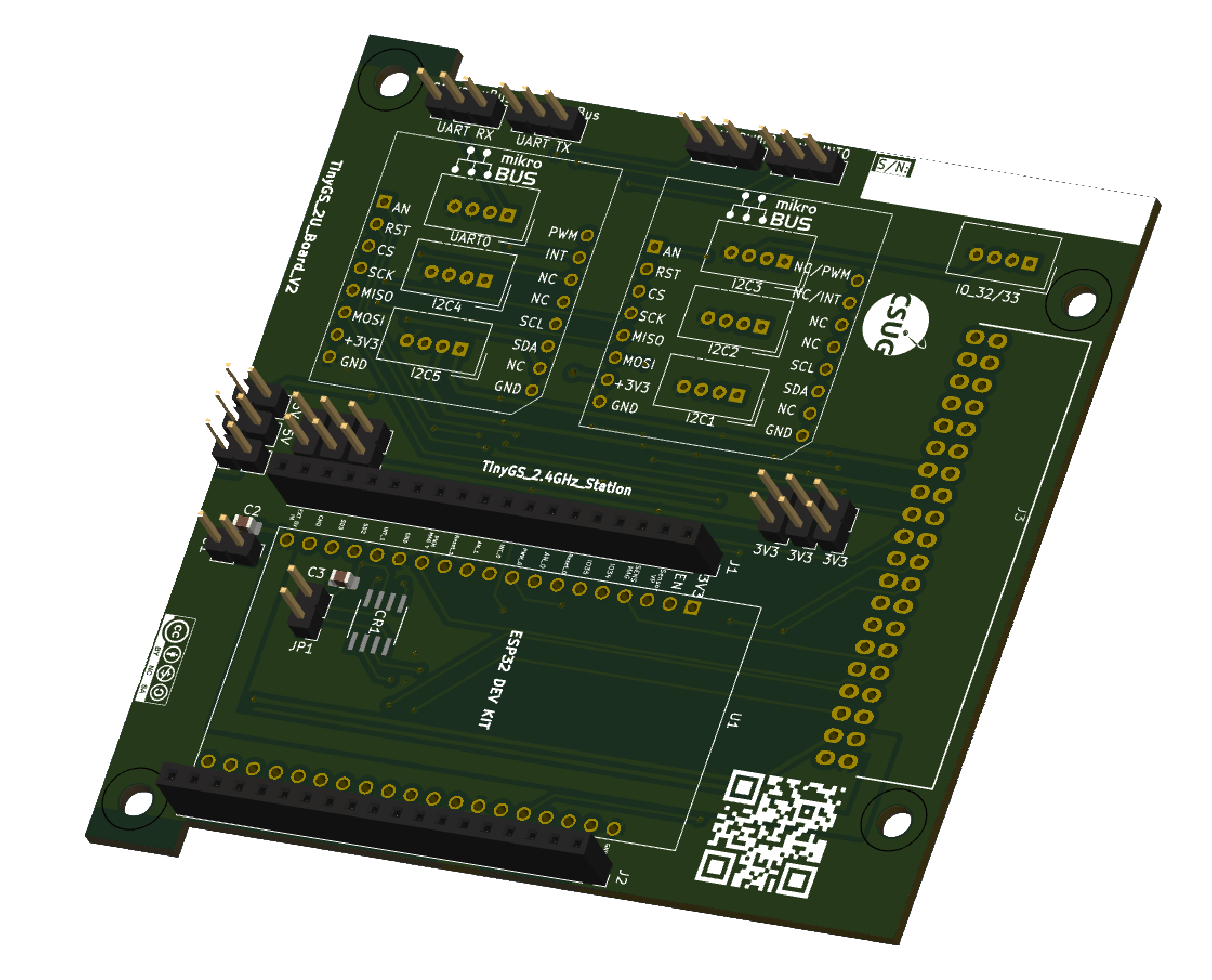
This board is the firts version of the LoRa 2.4GHz gateway for TinyGS.
Contain Schematic and PCB file for ESP32 Vroom + 2 Mikrobus modules + 2 groves connectors (RXTX,I2C).
This Board is designed to support a ESP32 devkitC-V4 and 2 MiKroBus modules. This board is the firts version of the 2.4GHz tinygs ground station gateway and named Board_V2
The purpose of this board is to control mikrobus modules including SX1280 technology that will transmit and receive messages on a 2.4GHz radio frequency. Each module are connected to a ESP32 which will be connected to the wifi.
Mikrobus board is an add-on board socket standard made by mikroe
Connection between ESP32 - ESP32-DevKitC V4 and Mikrobus modules
MiKroBus 0:
SPI_0:
CLK 	IO18
MISO	IO19
MOSI	IO23
NSS(CS)	IO05

UART_0	:
Tx	NC
Rx	NC

I2C:
SDA	IO21
SCL	IO22

AN_0	IO33
RESET_0 IO32
PWM_0	IO25
INT_0	IO26
MiKroBus 1:
SPI_0
CLK 	IO18
MISO	IO19
MOSI	IO23
NSS 	IO15

UART_2
Tx	IO17
Rx	IO16

I2C:
SDA	IO21
SCL	IO22

AN_1	IO27
RESET_1 IO14
PWM_1	IO04
INT_1	IO13
Grove connector available on board :
I2C:			UART_2(Rx/Tx):		GPIO(INPUT Only):
SDA   IO21		Tx	IO17		IO34
SCL   IO22		Rx	IO16		IO35
UART_2 can be connected to module MiKroBus 2 or to grove connector. A jumper need to be plug to choose beetween grove output or the mikrobus module.
Two UFL connected to a SMA mount edge connector are available to plug an antenna. They are disconnected from the rest of the board, which allows to connect the module that you want to the antenna, with a SMA -UFL connector.
A powerbank can be plug under the board to supply the 3V. The powerbank is design for ESP32 and is purchasable on amazon. 5V is only available on the Mikrobus 1 module.
Careful:
Lib & empreinte folder contains all necessary symbol and footprint for the project:
| Qty | Value | Footprint | References |
|---|---|---|---|
| 10 | 0 | Resistor_SMD:R_0805_2012Metric_Pad1.20x1.40mm_HandSolder | R6, R7, R8, R9, R10, R11, R12, R13, R14, R15 |
| 7 | 100n | Capacitor_SMD:C_0805_2012Metric_Pad1.18x1.45mm_HandSolder | C3, C4, C5, C6, C8, C9, C10 |
| 4 | 4K7 | Resistor_SMD:R_0805_2012Metric_Pad1.20x1.40mm_HandSolder | R1, R2, R3, R4 |
| 3 | 10u | Capacitor_SMD:C_0805_2012Metric_Pad1.18x1.45mm_HandSolder | C1, C2, C7 |
| 3 | I2C_Grove | Connector:NS-Tech_Grove_1x04_P2mm_Vertical | J4, J6, J9 |
| 2 | Conn_01x15 | Connector_PinHeader_2.54mm:PinHeader_1x15_P2.54mm_Vertical | J2, J7 |
| 2 | LOGO | Com_L432KC_footprint:logo_csug | G***, G*** |
| 1 | |||
| 1 | Bus Standard | Com_L432KC_footprint:flatsat_conn | J1 |
| 1 | INT_SEL | Connector_PinHeader_2.54mm:PinHeader_1x03_P2.54mm_Vertical | JP5 |
| 1 | L9616 | Package_SO:SO-8_3.9x4.9mm_P1.27mm | CR1 |
| 1 | LOGO | Logos-image:mikrobus_logo | G*** |
| 1 | LOGO | Com Nucleo library:qr_code_flatsat | QR |
| 1 | MCP9808_MSOP | Package_SO:MSOP-8_3x3mm_P0.65mm | U2 |
| 1 | MCU | Module:Arduino_Nano | L432KC1 |
| 1 | MIKROE-4247 | Com_L432KC_footprint:MIKROE4247 | J5 |
| 1 | PCI_EXPRESS_CARD | Connector_PCBEdge:BUS_PCI_Express_Mini | IC1 |
| 1 | PWM1_SEL | Connector_PinHeader_2.54mm:PinHeader_1x03_P2.54mm_Vertical | JP1 |
| 1 | RX_SEL | Connector_PinHeader_2.54mm:PinHeader_1x03_P2.54mm_Vertical | JP3 |
| 1 | Reset | Button_Switch_THT:SW_PUSH_6mm | SW1 |
| 1 | TX_SEL | Connector_PinHeader_2.54mm:PinHeader_1x03_P2.54mm_Vertical | JP4 |
| 1 | speed_controller | Connector_PinHeader_2.54mm:PinHeader_1x02_P2.54mm_Vertical | JP2 |
The 46 most common of 47 parts.


Nuclear-Squid/KiCad-Templates
A KiCad plugin to save and reuse schematic + routing templates.


VoronDesign/Voron-Hardware
Cool Hardware designed by the Voron Design group

hackclub/OnBoard
💡 Join 1,000 teenagers and make your first PCB with a $100 grant!


It measures 90 × 92 mm and has 2 copper layers, 1.6 mm thick.
47 parts, built around the L9616 and MIKROE-4247. The full list of its parts is on this page, with links to each part's symbol and footprint where PCBKit's library has them.
From the csu-grenoble/flatsat repository on GitHub, at the commit this page was made from: the board is Hardware/Thingsat_INISAT/Projet Kicad/Com_Nucleo-L432kc.kicad_pcb and its schematic Hardware/2U-PCB-OBC_L476RG/OBC_L476RG/OBC_L476RG.kicad_sch. PCBKit opens the board in the browser, with nothing to install.
Its repository states no licence, so its author keeps all rights: ask csu-grenoble before reusing the design.