Skip to the content
PCBKitNew board
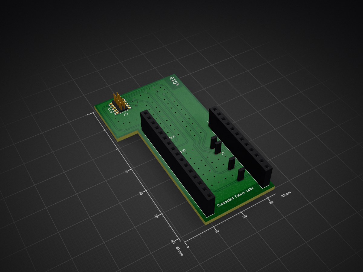
2 layers33 × 61 mmCFL EE FeatherDebugShield, the printed circuit board in 3D

Shield to connect JTAG pins on Feather M0

Size
33 × 61 mm
Copper layers
2
Thickness
1.6 mm
Parts
9
Nets
34
Pads
60
Tracks, vias
66, 79
Pours
2
Routed
Yes
KiCad
KiCad 7 (file 20221018)
Created
23 Oct 2023
Updated
8 Dec 2023

Overview

CFL EE FeatherDebugShield is an open-source printed circuit board by connectedfuturelabs, from the connectedfuturelabs/CFL_EE_FeatherDebugShield repository on GitHub, published under the MIT licence. It is a 2-layer board of 33 × 61 mm with 9 parts on 34 nets, routed with 66 tracks and 79 vias.

README

README.md

Description

  • This is a SWD breakout shield for the Feather M0 and a JTAG breakout shield for Feather ESP32.
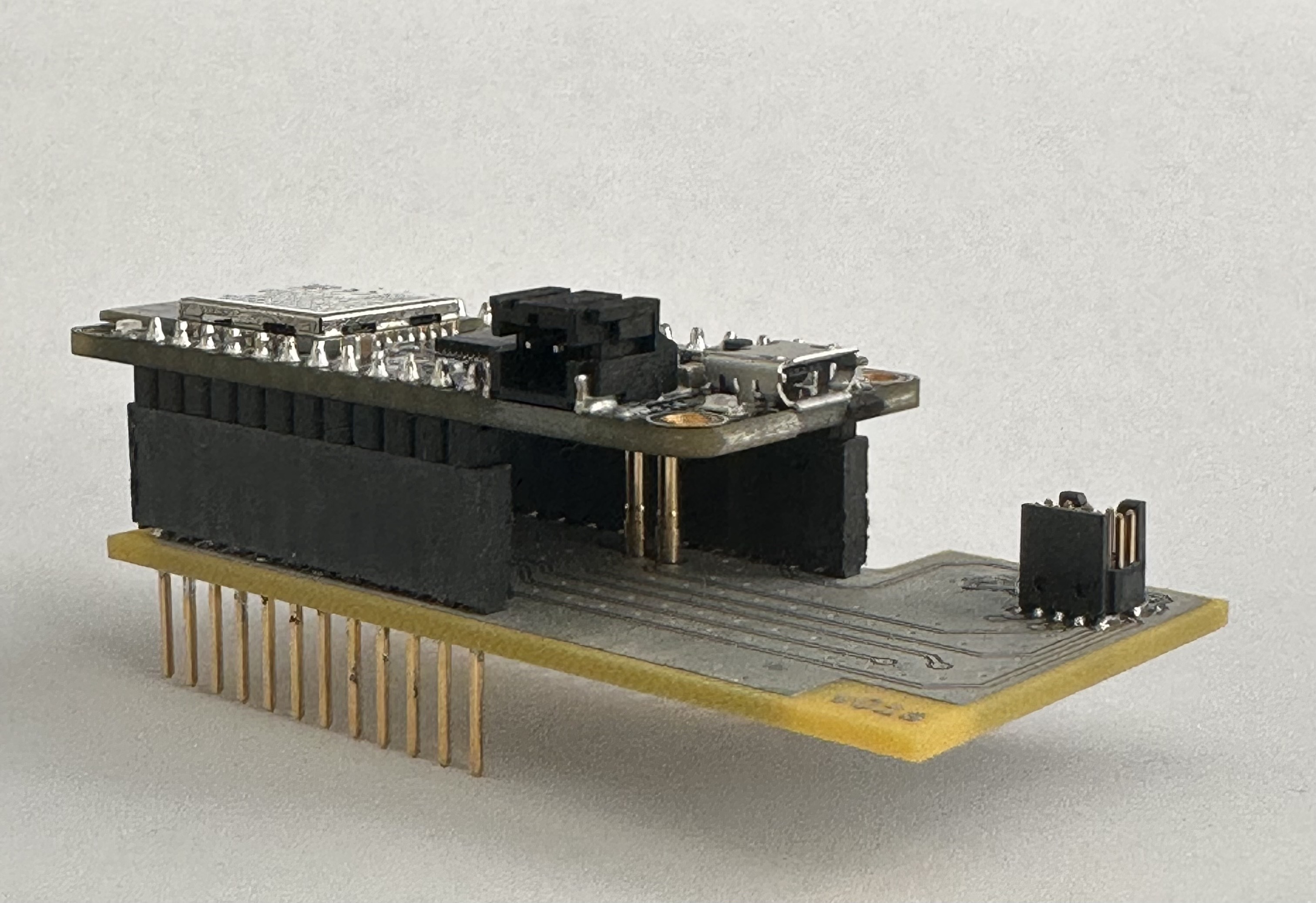
  • The Feather M0 has a provision for SWD debugging which requires soldering leads to the SWD pads on the bottom on the Feather M0. We made this shield so that we can debug a Feather M0 without having to solder leads. Instead, we use pogo pins to create the contact when the feather M0 is stacked on this shield.
  • The Feather ESP32 can be debugged using the JTAG interface. This shield has a provision for debugging with ESP32 using solder bridges to create the necessary connections. This configuration has not been tested.

Debug shield

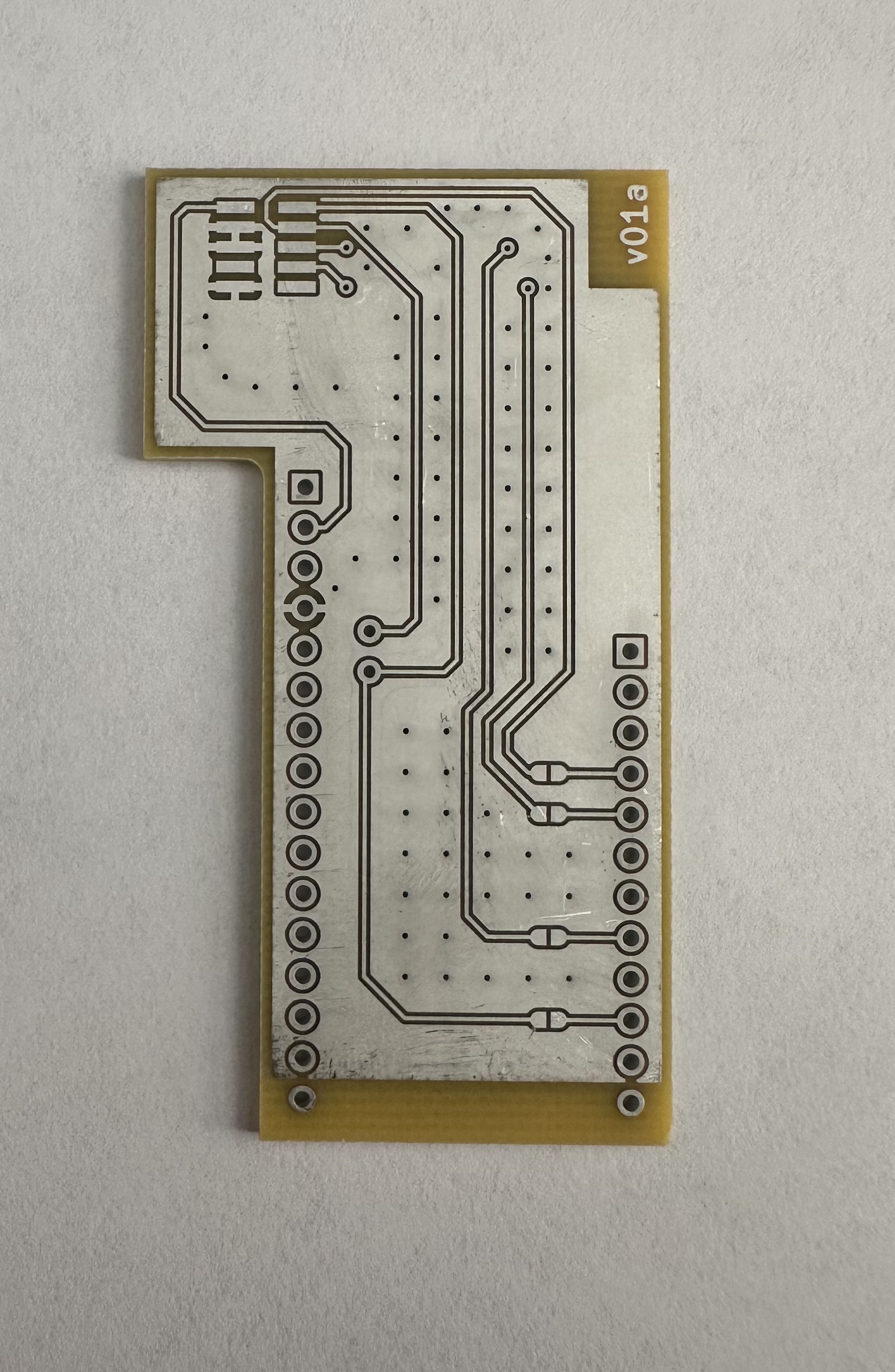
Note that this is a bare bones board (which is why the SM and silk screen are missing)

stagehow it looks
After fabrication
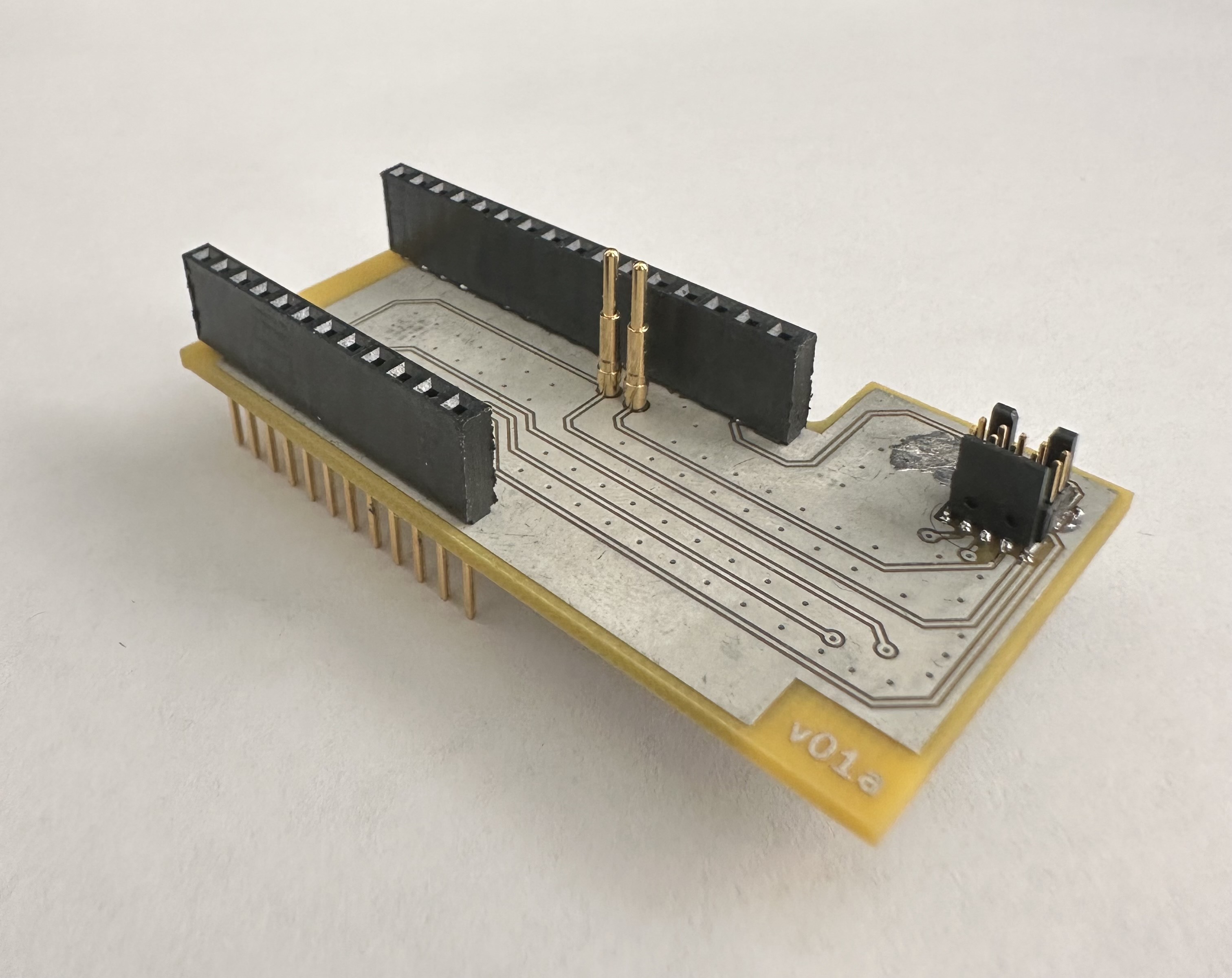
After Assembly
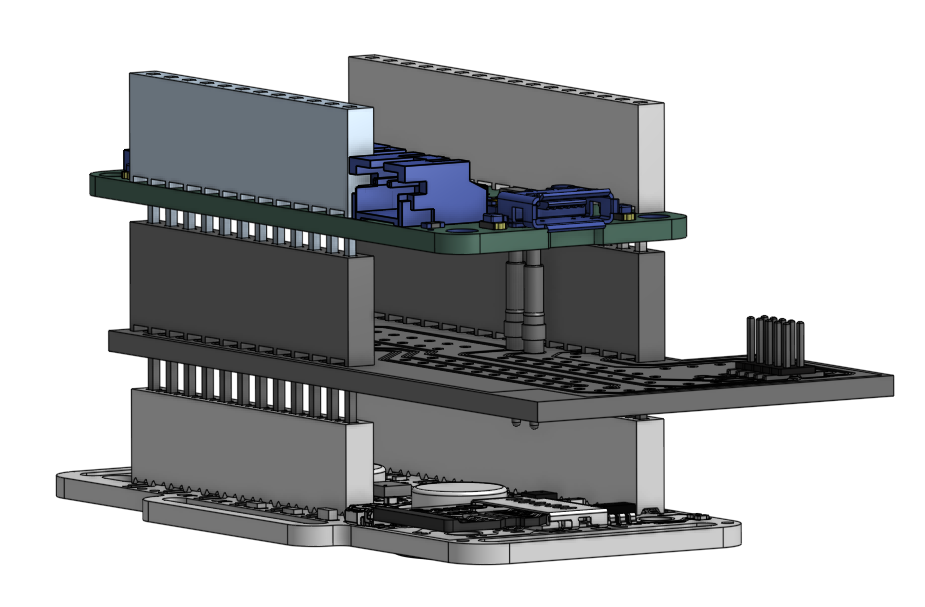
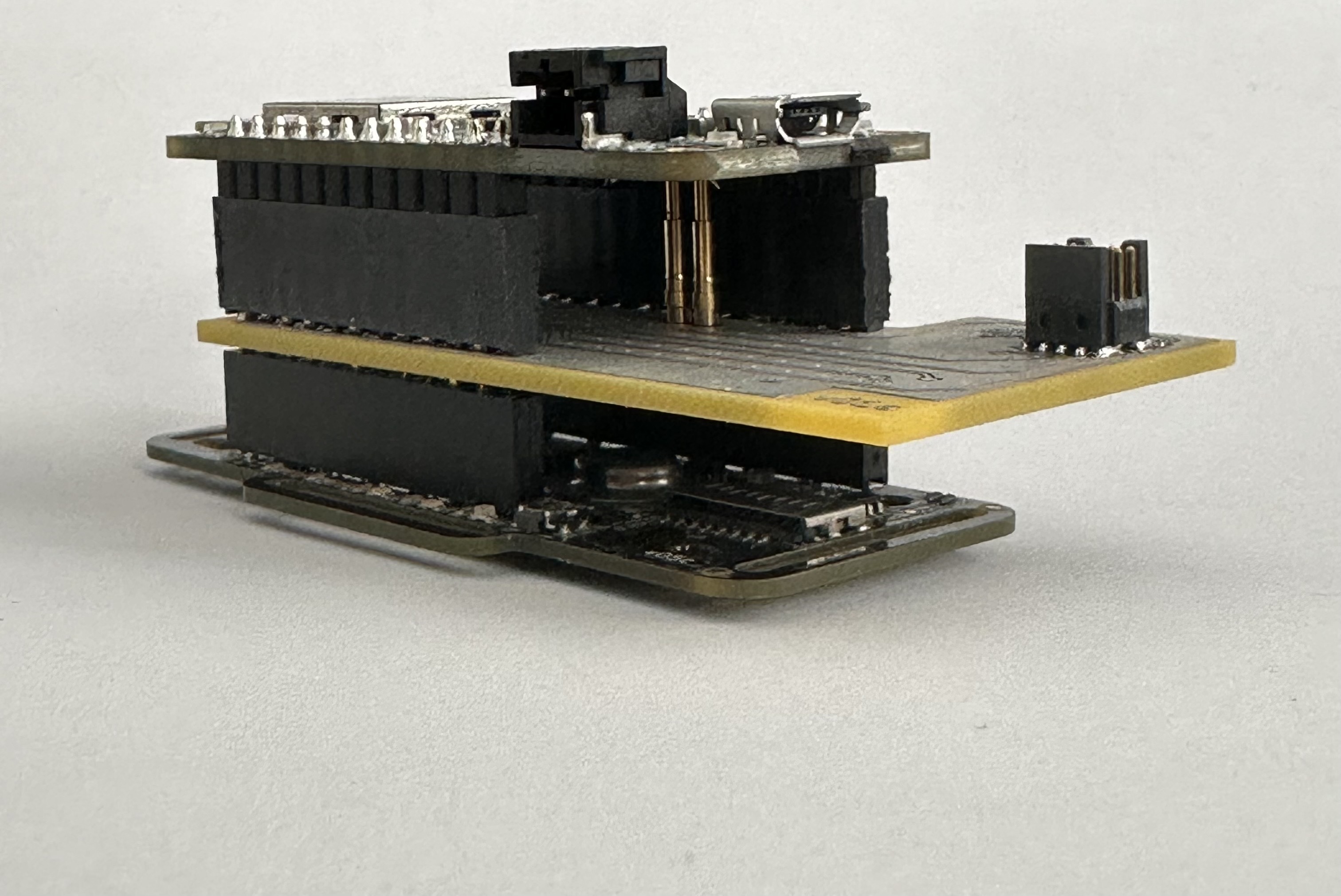
Stacked with a Feather
Stacked with Feather and EmotiBit

Using this repository

  • The latest release contains all files required for creating the board.
  • To fabricate this board
    • Download the .zip from the release page.
    • The files needed for manufacturing are in the Gerbers folder.
    • Just upload the gerber design files on a manufacturer's website and choose other board specifications.
    • We used 4PCB as our manufacturer.
    • The _bom.csv file contains the parts needed for assembly. You can directly upload the bom file into the digikey portal to get the required parts for assembly.
  • Once the shield is fabbed and stacked, you can use the 10 pin JTAG conector cable to connecto to a J-Link debugger.

Assembly notes

  • It is important to line up the pogo pins vertically to ensure there is a contact with the pads on the Feather. The following sequence helps with the allignment:
    • solder the 12 and 16 pin connector.
    • place the pogo pins in the correct position
    • stack the Feather on the shield.
    • then align the pogo pins with a pair of tweezers to ensure contact.
    • solder the pins in place
  • We used stacking headers because we intend to use this as a triple stack with EmotiBit, but if you are only interested in debugging the Feather, then you can use normal female socket for the connector.

Additional Notes

  • The design was created in Kicad 7.
  • If you want to build on top of this design, please feel free to fork the repository and make the rewuired changes! you will need to download Kicad v7+ to work with the design files.

Parts

9
QtyValueFootprintReferences
4CONN_JUMPER_NOCFL_EE_BioSensor_Lib_FP:CONN_SLDR_BRDG_NOJ3, J7, J8, J9
1Conn_01x12Connector_PinSocket_2.54mm:PinSocket_1x12_P2.54mm_VerticalJ1
1Conn_01x16Connector_PinSocket_2.54mm:PinSocket_1x16_P2.54mm_VerticalJ2
1Conn_ARM_JTAG_SWD_10CFL_EE_KiCad_Lib:SAMTEC_FTSH-105-01-F-DV-K-TRJ4
1SWCLKCFL_EE_BioSensor_Lib_FP:CONN_PROBE_SPRING_01X01_C150H75J6
1SWDIOCFL_EE_BioSensor_Lib_FP:CONN_PROBE_SPRING_01X01_C150H75J5

Questions

How big is the CFL EE FeatherDebugShield PCB?

It measures 33 × 61 mm and has 2 copper layers, 1.6 mm thick.

What parts does the CFL EE FeatherDebugShield use?

9 parts. The full list of its parts is on this page, with links to each part's symbol and footprint where PCBKit's library has them.

Where can I download the CFL EE FeatherDebugShield KiCad files?

From the connectedfuturelabs/CFL_EE_FeatherDebugShield repository on GitHub, at the commit this page was made from: the board is CFL_EE_FeatherDebugShield.kicad_pcb and its schematic CFL_EE_FeatherDebugShield.kicad_sch. PCBKit opens the board in the browser, with nothing to install.

Can I use the CFL EE FeatherDebugShield design in my own project?

Its repository publishes it under the MIT licence: you may reuse it on that licence's terms (keep the author's notice, and for a copyleft licence share your changes alike).

Similar boards

  • 2 layers103 × 30.5 mmTS Back Endcap, the printed circuit board in 3D

    TS Back Endcap

    EEVengers/ThunderScope

    ThunderScope GitHub Repo

    9 parts1.3kMIT
  • 2 layers31.8 × 47.6 mmNGC 38 connector, the printed circuit board in 3D

    NGC 38 connector

    rusefi/rusefi

    rusefi - GPL internal combustion engine control unit

    9 parts1.2k
  • 2 layers24 × 27.3 mmExpansion Card Retrofit, the printed circuit board in 3D

    Expansion Card Retrofit

    FrameworkComputer/ExpansionCards

    Reference designs and documentation to create Expansion Cards for the Framework Laptop

    9 parts1.1kCC-BY-4.0
  • 2 layers15.6 × 17.3 mmSKR Mini TFT Thermistor Board, the printed circuit board in 3D

    SKR Mini TFT Thermistor Board

    VoronDesign/Voron-Hardware

    Cool Hardware designed by the Voron Design group

    9 parts1.1kGPL-3.0
  • 2 layers39.1 × 49.5 mmLearnoliver, the printed circuit board in 3D

    Learnoliver

    hackclub/OnBoard

    💡 Join 1,000 teenagers and make your first PCB with a $100 grant!

    9 parts915
  • 2 layers17.4 × 16.9 mmToolhead, the printed circuit board in 3D

    Toolhead

    tanaes/whopping_Voron_mods

    9 parts787GPL-3.0
  • 2 layers9.8 × 108 mmExpander, the printed circuit board in 3D

    Expander

    wntrblm/Castor_and_Pollux

    A Juno-inspired dual oscillator

    9 parts587
  • 2 layersKeyboard after, the printed circuit board in 3D

    Keyboard after

    adamws/kicad-kbplacer

    KiCad plugin for automatic keyboard's key placement and routing

    9 parts547GPL-3.0