2 layers48.3 × 26.7 mm
 ColdeZhang/Kernel_Board3
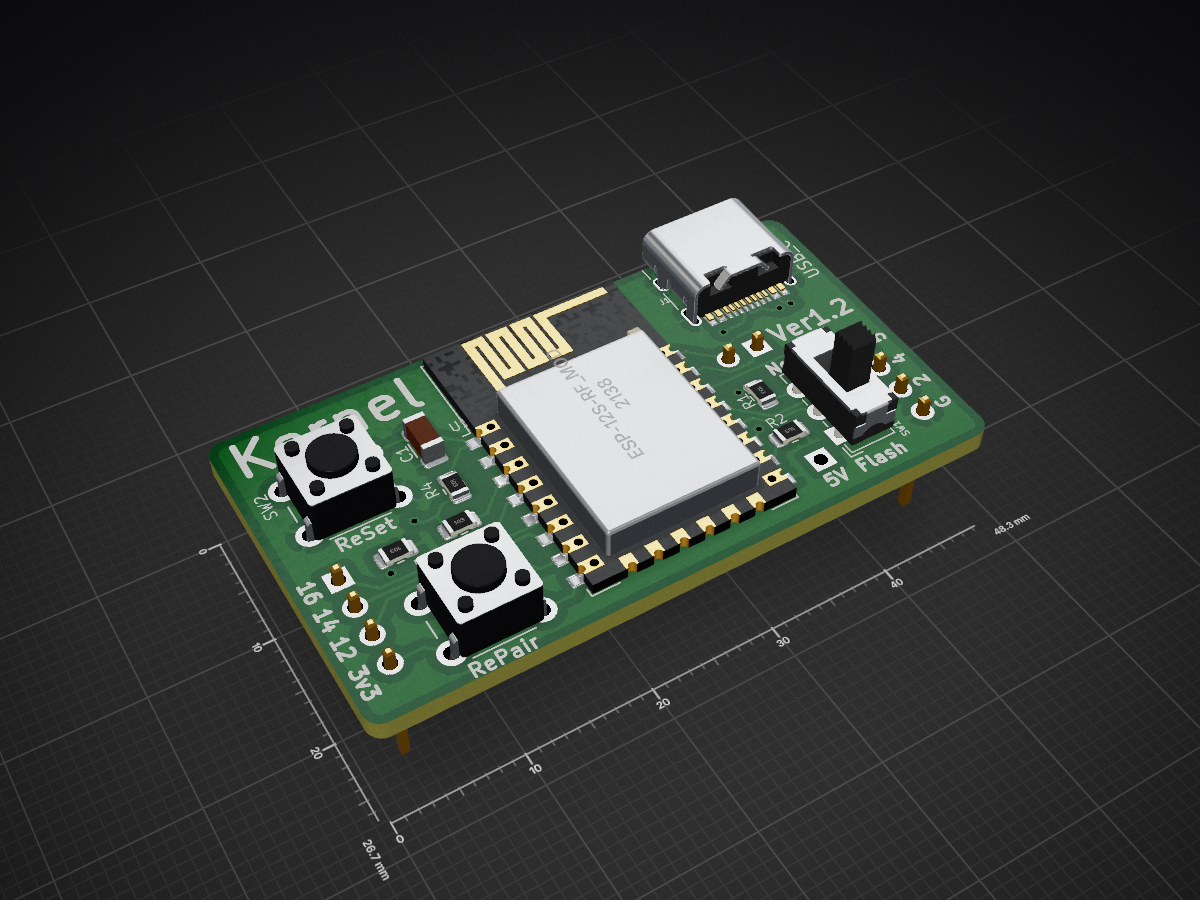
Kernel is an open-source printed circuit board by ColdeZhang, from the ColdeZhang/Kernel_Board repository on GitHub. It is a 2-layer board of 48.3 × 26.7 mm with 19 parts on 33 nets, routed with 163 tracks and 11 vias.
It is built around the CH340C and AMS1117-3.3. Its parts include 5 resistors, 5 connectors, 3 capacitors, 3 ICs and 3 switches. It belongs with the ESP8266 boards of this library.


Kernel板主要基于安信可的ESP-12S(后者基于乐鑫ESP8266),为HomeKit智能家居开发准备了一些基础电路。因此更适合没有太多电路基础的新手着手进行Homekit智能家居的开发。相比于ESP-01在保留必须的一部分功能后尽可能的引出了更多的可用IO口(6个),使之可以适应更复杂的项目开发,并且拥有更加稳定的网络连接。项目基于Apple Homekit与ESP8266,并且全部开源。
该核心板全部文件托管在:Github仓库
该核心板配套的代码教程参见:ESP8266-Homekit 模板代码
该核心板配套的扩展版系列目前有:??、??、??、??
在0.1版本中Flash(烧写)模式被称为Upload(上传)模式
从1.0版本开始新增USB-Type-C接口支持供电+烧写程序,无需外接TTL转USB
Reset按键可以实行一键重启,免除了切换模式时需要拔插电源重启的麻烦。
由于ESP-12S具有两种模式(运行模式与烧写模式),并且需要通过将IO0接地来手动切换。本核心板将此操作使用一个单刀双掷开关(SW1)集成在主板上,可以通过拨动开关一键切换运行模式(Normal)和烧写模式(Flash)。
因为配对信息是被写入在ESP-12S的闪存中的,所以通过Reset是无法擦除配对记录来重新配对的。如果需要重新配对需要调用Apple Homekit内置函数来执行闪存内信息的重写,在本核心板配套的Template代码中,该功能已被写在了IO13引脚上。硬件层面通过一个按钮RePair,按下即可重新配对。
该核心板拥有恰到好处的尺寸(宽5cm),使其恰好能够放入一个常规开关盒中,十分适合用来制作一些实用的智能家居设备。而从成本(一般来说越小的元件价格越高)与加工难度(越复杂的电路加工难度越大)的角度考虑,并没有将其做的十分小巧的必要。
将右下的开关选择至Normal,在任意的一个3V3引脚上连接3.3v的直流正极,任意一个GND引脚连接相应的负极即可启动开发板。在开发中如果需要重启开发板,不需要断开电源重连,可以直接按下主控板上的Reset按键执行重启。(该操作不会擦除ESP-12S上内存与闪存的数据)
将右下的开关选择至Flash,按下Reset按钮执行重启,重启后主控板处于烧写模式。
将USB转TTL串口烧写器的对应引脚连接至开发板右上一排引脚TX、RX、3V3、GND,再将烧写器连接至电脑,即可从电脑烧写程序至开发板。烧写完成后需要将开关切换回Normal模式,再按下重启按钮。
将USB-Type-C数据线连接至核心板,另一段连接至电脑,即可从电脑烧写程序至开发板。烧写完成后需要将开关切换回Normal模式,再按下重启按钮。

略

| Qty | Value | Footprint | References |
|---|---|---|---|
| 5 | 10k | Resistor_SMD:R_0805_2012Metric | R1, R2, R3, R4, R5 |
| 3 | 10uF | Capacitor_SMD:C_1206_3216Metric | C1, C2, C3 |
| 1 | AMS1117-3.3 | Package_TO_SOT_SMD:SOT-223-3_TabPin2 | U3 |
| 1 | CH340C | Package_SO:SOIC-16_3.9x9.9mm_P1.27mm | U2 |
| 1 | Conn_01x01_Male | Connector_PinHeader_2.54mm:PinHeader_1x01_P2.54mm_Vertical | J5 |
| 1 | ESP-12S-RF_Module | RF_Module:ESP-12E | U1 |
| 1 | L | Connector_PinHeader_2.54mm:PinHeader_1x04_P2.54mm_Vertical | J2 |
| 1 | MODE | Button_Switch_THT:SW_E-Switch_EG1271_DPDT | SW1 |
| 1 | R | Connector_PinHeader_2.54mm:PinHeader_1x04_P2.54mm_Vertical | J3 |
| 1 | RePair | Button_Switch_THT:SW_PUSH_6mm_H4.3mm | SW3 |
| 1 | ReSet | Button_Switch_THT:SW_PUSH_6mm_H4.3mm | SW2 |
| 1 | TTL | Connector_PinHeader_2.54mm:PinHeader_1x02_P2.54mm_Vertical | J4 |
| 1 | USB_C_Receptacle_USB2.0 | Connector_USB:USB_C_Receptacle_HRO_TYPE-C-31-M-12 | J1 |
It measures 48.3 × 26.7 mm and has 2 copper layers, 1.6 mm thick.
19 parts, built around the CH340C and AMS1117-3.3. The full list of its parts is on this page, with links to each part's symbol and footprint where PCBKit's library has them.
From the ColdeZhang/Kernel_Board repository on GitHub, at the commit this page was made from: the board is Ver_1_X/Kernel.kicad_pcb. PCBKit opens the board in the browser, with nothing to install.
Its repository states no licence, so its author keeps all rights: ask ColdeZhang before reusing the design.


SRA-VJTI/sra-board-hardware-design
ESP32-based Development Board for Robotics and Embedded Applications


ricardoquesada/unijoysticle2
Bluetooth gamepad support for the Commodore 64 / Atari / Amiga, etc.


