
4 layers308 × 225.4 mm

 codepainters/e800j16
Elwro 800 Junior replica
Ports pcb is an open-source printed circuit board by codepainters, from the codepainters/e800j repository on GitHub. It is a 2-layer board of 308 × 53.1 mm with 95 parts on 76 nets, routed with 398 tracks and 68 vias.
It is built around the BC557. Its parts include 57 connectors, 6 resistors, 2 switches, 1 capacitor and 1 fuse.
This part of the project is the exact clone of the original Elwro 800 Junior PCB revision C. The PCB was reverse engineered from scanned images of the original PCB. All dimensions and mounting holes placements have been preserved, so the board can be used as a replacement for the original one.
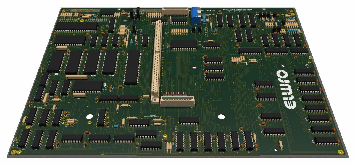
Note: Read this README file carefully, it contains some important assembly instructions!
This directory contains the KiCAD 9 project, plus:
For files to be programmed into EPROMs, see here.
Note: KiCAD PCB file still embeds the scanned images used for reverse engineering, so don't be surprised by the file size! The project passes PCB vs schematic parity check.
Schematics:
MEMR, or IOR) are only connected using labels, as the wires would clutter the drawing too much otherwise.+ or - sign for active-high (e.g. +RELOK) and active-low (e.g. -MEMR) signals, respectively. My schematic diagrams use standard notation with active-low signals with a bar above the name.J16, I5, etc. I decided to use standard U1, U2, ... numbering, but original reference designators are stored as OrigRef attribute (also visible in the PCB editor in User.Comments layer).E48 series resistors for no good reason (most likely because of availability), my replica uses standard 5% E24 series resistors. Original values are stored in the schematic as OrigValue attributes.OrigType attribute for cross-reference.PCB:
In1.Cu and In2.Cu layers (typically used for 4-layer PCB projects).There are two variants of the Gerber files available:
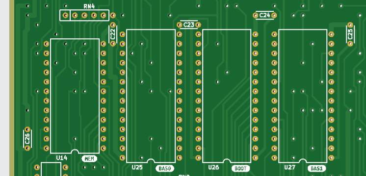
e800j_rev_c_v1.1.zip - a "modern" one, with tented vias and silkscreen (on both sides of the board!) - most likely what you want. The board manufactured from this set of files looks like this:
e800j_rev_c_v1.1_retro.zip - a "retro" variant, without via tenting and silkscreen, which aims to look as much like the original PCB as possible (which might be useful for restoration projects):
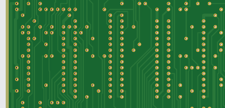
Unless you specifically need the retro variant, I highly recommend the standard one, with tented vias and silkscreen - it makes assembly much easier.
Most of the parts used on the board are standard TTL 74xx chips, with some exceptions:
74S474 512x8 PROM memories, used in the I/O and memory address decoders, are hard to find and difficult to program. As part of the project, I've prepared two replacement options:
e800j_addr_dec_gal - using GAL16V8 PLD
e800j_addr_dec_atf - using ATF1502ASL (if you prefer SMD chips)
Both options have been verified to work properly.
The 2716 EPROM (U11 on the schematics, used to generate video signal timing) can be replaced with a 2732 memory (with the content doubled, see roms for the appropriate file).
Some chips required replacement:
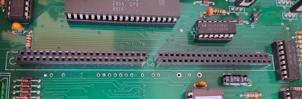
U1 - I had to replace a perfectly valid 74LS04 with another brand, as it didn't want to oscillate, eventually I got it working with a UCY74LS04 from Cemi. Similarly, I had to replace the U4 chip (74LS04) with UCY74LS04 as well. These chips work in specific, semi-analog circuits, so the choice of actual chips might be important.U28..U31 (perfectly valid Motorola 74LS153 address multiplexers) with SN74LS153N from Texas Instruments solved the issue, and virtually every 4164 DRAM chip I could find works properly now.for GT1 connector (used to plug-in floppy disk controller), you can use original Eltra 841 84-pin socket, if available. This is the recommended way if you want to use the original FDC (or a clone with an Eltra plug). Otherwise simple pin-header sockets will do (and pin headers work with Eltra 841 too. My future expansion PCBs are going to use pin headers):
for keyboard connectors ( W1 and W2 ) one can use standard pin headers (10-pins long) - it works well with Eltra plugs.
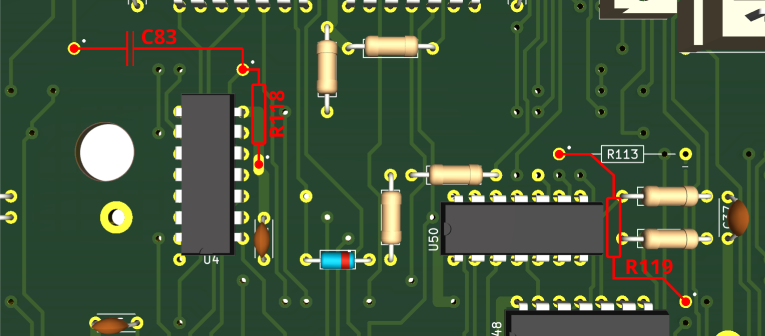
I decided to fully replicate the original factory mods, to better match the look and feel of the PCB.
Changes involve:
C83 (120pF) and R118 (510 ohm)R119 (100 ohm)The soldering points are marked with small dots on the silkscreen layer:
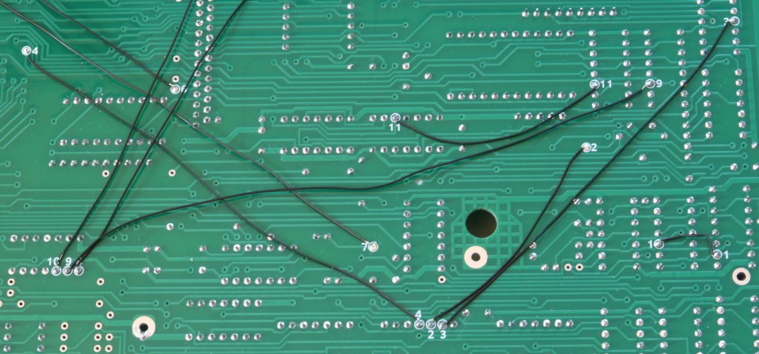
Finally, 11 wire connections are needed on the bottom of the PCB. Soldering points are numbered - connect 1 to 1, 2 to 2 and so on.
If assembled from functional parts, the board requires no tuning and should work from the first power-up.
J51). If you can't get properly synchronized video, double-check U19 (2716 EPROM responsible for generating video timing signals). Some programmers (including my TL866A) are known to be occasionally problematic with 2716 memories, what sometimes helps is programming the memory twice (without erasing).U1 and U4 chips might need replacement (see parts section above), in case of issues it's best to check the clock signals with an oscilloscope.U28..U31 (again, see above for explanation).That's all, folks!
| Qty | Value | Footprint | References |
|---|---|---|---|
| 39 | Conn_01x01_Socket | Connector_PinHeader_2.54mm:PinHeader_1x01_P2.54mm_Vertical | J1, J2, J3, J10, J14, J15, J16, J17, J18, J19, J20, J21, J22, J23, J24, J30 +23 |
| 5 | 4k7 | Resistor_THT:R_Axial_DIN0207_L6.3mm_D2.5mm_P10.16mm_Horizontal | R1, R2, R3, R4, R5 |
| 5 | BC557 | Package_TO_SOT_THT:TO-92_Inline | T1, T2, T3, T4, T5 |
| 5 | mth32 | e800j_custom:mth32 | MH2, MH3, MH4, MH6, MH7 |
| 4 | ~ | Connector_PinHeader_2.54mm:PinHeader_1x01_P2.54mm_Vertical | J37, J38, J39, J40 |
| 3 | , , | ||
| 3 | Conn_01x01_Socket | ports_pcb:pin24 | J11, J12, J13 |
| 2 | G*** | kibuzzard-67F911F0 | kibuzzard-67F911F0, kibuzzard-67F911F0 |
| 2 | Junet | ports_pcb:CUI_SDS-50J | J104, J105 |
| 2 | mth25 | e800j_custom:mth25 | MH1, MH5 |
| 1 | 0R* | Resistor_THT:R_Axial_DIN0207_L6.3mm_D2.5mm_P10.16mm_Horizontal | R6 |
| 1 | 100nF | Capacitor_THT:C_Disc_D5.0mm_W2.5mm_P2.50mm | C1 |
| 1 | 2A | Fuse:Fuseholder_Clip-5x20mm_Littelfuse_445-030_Inline_P20.50x5.20mm_D1.30mm_Horizontal | F1 |
| 1 | 5V/2A | Connector_BarrelJack:BarrelJack_GCT_DCJ200-10-A_Horizontal | J107 |
| 1 | Conn_01x02 | Connector_Molex:Molex_KK-254_AE-6410-02A_1x02_P2.54mm_Vertical | J108 |
| 1 | FON | Connector_PinHeader_2.54mm:PinHeader_1x02_P2.54mm_Vertical | JP4 |
| 1 | G*** | kibuzzard-67F91771 | kibuzzard-67F91771 |
| 1 | G*** | kibuzzard-67F9119B | kibuzzard-67F9119B |
| 1 | G*** | kibuzzard-67F8F98E | kibuzzard-67F8F98E |
| 1 | G*** | kibuzzard-67F91269 | kibuzzard-67F91269 |
| 1 | G*** | kibuzzard-67F911BA | kibuzzard-67F911BA |
| 1 | G*** | kibuzzard-67F91296 | kibuzzard-67F91296 |
| 1 | Joy_P8 | Connector_PinHeader_2.54mm:PinHeader_1x03_P2.54mm_Vertical | JP1 |
| 1 | Joystick | Connector_Dsub:DSUB-9_Pins_Horizontal_P2.77x2.84mm_EdgePinOffset7.70mm_Housed_MountingHolesOffset9.12mm | J100 |
| 1 | Power | ports_pcb:PS-22F03 | SW2 |
| 1 | Printer | Connector_Dsub:DSUB-25_Socket_Horizontal_P2.77x2.84mm_EdgePinOffset7.70mm_Housed_MountingHolesOffset9.12mm | J102 |
| 1 | RESET1 | e800j_custom:pin | J41 |
| 1 | RESET2 | e800j_custom:pin | J42 |
| 1 | RGB | Connector_Dsub:DSUB-9_Socket_Horizontal_P2.77x2.84mm_EdgePinOffset7.70mm_Housed_MountingHolesOffset9.12mm | J101 |
| 1 | Reset | ports_pcb:PS-22F03 | SW1 |
| 1 | SynH | Connector_PinHeader_2.54mm:PinHeader_1x03_P2.54mm_Vertical | JP2 |
| 1 | SynV | Connector_PinHeader_2.54mm:PinHeader_1x02_P2.54mm_Vertical | JP3 |
| 1 | Tape | ports_pcb:CUI_SDS-50J | J106 |
| 1 | Video | ports_pcb:CUI_SDS-50J | J103 |
| 1 | logo | ports_pcb:logo | IMG1 |
It measures 308 × 53.1 mm and has 2 copper layers, 1.6 mm thick.
95 parts, built around the BC557. The full list of its parts is on this page, with links to each part's symbol and footprint where PCBKit's library has them.
From the codepainters/e800j repository on GitHub, at the commit this page was made from: the board is ports_pcb/ports_pcb.kicad_pcb and its schematic e800j_rev_c/addr_dec.kicad_sch. PCBKit opens the board in the browser, with nothing to install.
Its repository states no licence, so its author keeps all rights: ask codepainters before reusing the design.


dotnet/iot
This repo includes .NET Core implementations for various IoT boards, chips, displays and PCBs.

ExploreEmbedded/8051_DevelopmentBoard
Design files and sample code for 8051 development Ultra Boards

robsonsmartins/usbflashprog
A memory device programmer (Flash/EPROM/E2PROM) board and software, connected to PC by USB port.

matthewcieplak/monotron-cv-adapter
A eurorack control voltage to Korg Monotron CV adapter board.


telec16/modular-synth
Little side project, don't expect much updates.
