2 layers103 × 30.5 mm

 codecooker1/Clickies
An extremely simple choc key fidget toy
Wiring Diagram is an open-source printed circuit board by codecooker1, from the codecooker1/Clickies repository on GitHub, published under the GPL-3.0 licence. It is a 2-layer board of 73.7 × 15.5 mm with 9 parts on 7 nets, routed with 14 tracks and 0 vias.
Its parts include 4 diodes, 4 switches and 1 resistor. It belongs with the keyboards and input boards of this library.
An extremely simple choc key fidget toy
This is an extremely easy and simple fidget toy. It only just really connects switches and LEDs. I'm using the standard cheap LEDs here cause they're really cheap and easy to find. While these LEDs doesn't fit under the choc keys by default but but but I can make it work by scraping a little bit of plastic from that hole. It works cause this doesn't interfere with the working mechanisms of the switch.
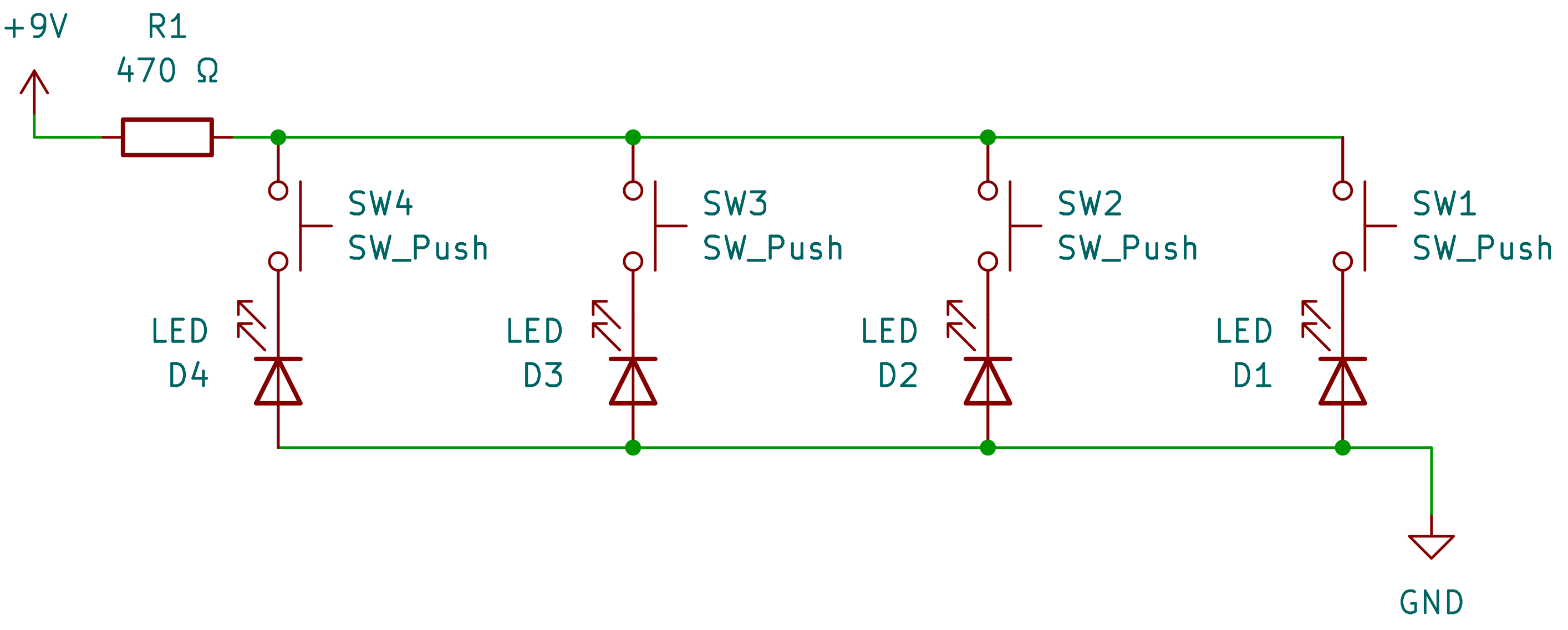
The circuit is also really simple and here's the wiring diagram:
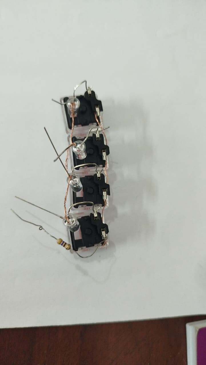
For the one I made I just peeled the insulator from a jumper wire and kind of connected the pins by wrapping the wire around them and pressing that with the hotswap socket.
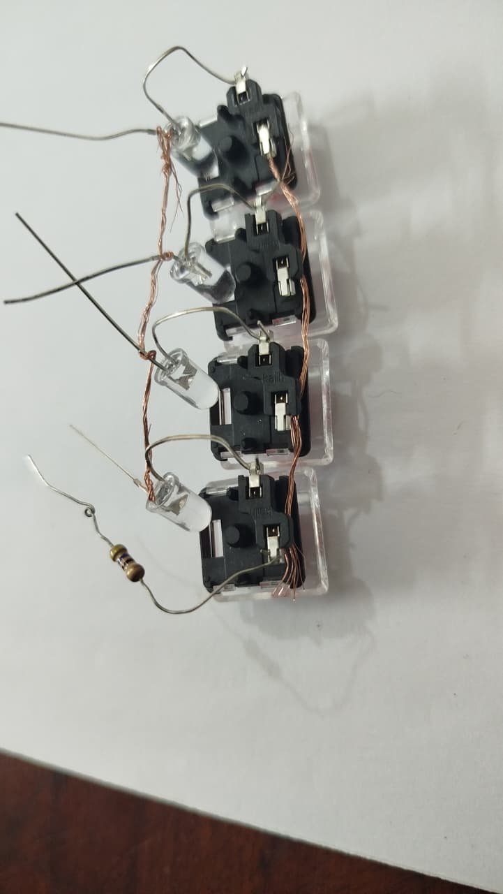
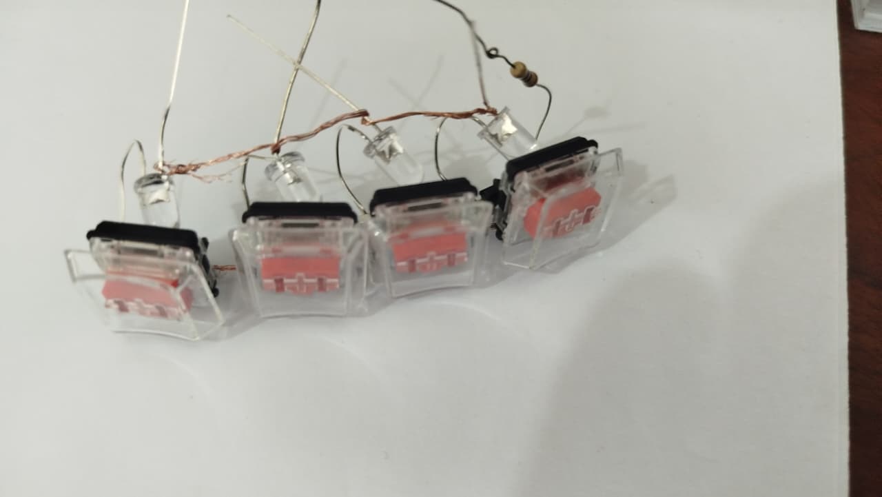
More Pics:
After finishing wiring I used air dry clay to keep everything together and make a nice little soft casing.
Here's how the current final version looks like:
https://github.com/user-attachments/assets/d40e0147-6267-40e9-9e10-2c23bf32484c
I know my clay skills suck and I even messed up some connections while making the clay casing but hey, it works!
Its honestly a tiny little bit more satisfying than I expected lol. Maybe I should make a better version of this in the future.
| Qty | Value | Footprint | References |
|---|---|---|---|
| 4 | LED | LED_THT:LED_D3.0mm | D1, D2, D3, D4 |
| 4 | SW_Push | PCM_marbastlib-choc:SW_choc_v1_HS_CPG135001S30_1u | SW1, SW2, SW3, SW4 |
| 1 | 470 Ω | Resistor_THT:R_Axial_DIN0207_L6.3mm_D2.5mm_P7.62mm_Horizontal | R1 |
It measures 73.7 × 15.5 mm and has 2 copper layers, 1.6 mm thick.
9 parts. The full list of its parts is on this page, with links to each part's symbol and footprint where PCBKit's library has them.
From the codecooker1/Clickies repository on GitHub, at the commit this page was made from: the board is Wiring_Diagram/Wiring_Diagram.kicad_pcb and its schematic Wiring_Diagram/Wiring_Diagram.kicad_sch. PCBKit opens the board in the browser, with nothing to install.
Its repository publishes it under the GPL-3.0 licence: you may reuse it on that licence's terms (keep the author's notice, and for a copyleft licence share your changes alike).


FrameworkComputer/ExpansionCards
Reference designs and documentation to create Expansion Cards for the Framework Laptop

VoronDesign/Voron-Hardware
Cool Hardware designed by the Voron Design group

hackclub/OnBoard
💡 Join 1,000 teenagers and make your first PCB with a $100 grant!


adamws/kicad-kbplacer
KiCad plugin for automatic keyboard's key placement and routing