
2 layers23.1 × 18 mm

 christrotter/multi-paddle-pcb
A single pcb for mk21 paddles, typewriter-esque.
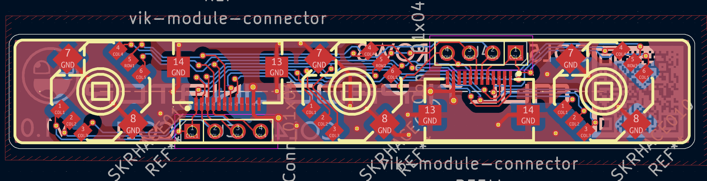
Multi paddle pcb is an open-source printed circuit board by christrotter, from the christrotter/multi-paddle-pcb repository on GitHub, published under the MIT licence. It is a 2-layer board of 60 × 10 mm with 9 parts on 15 nets, routed with 417 tracks and 61 vias.
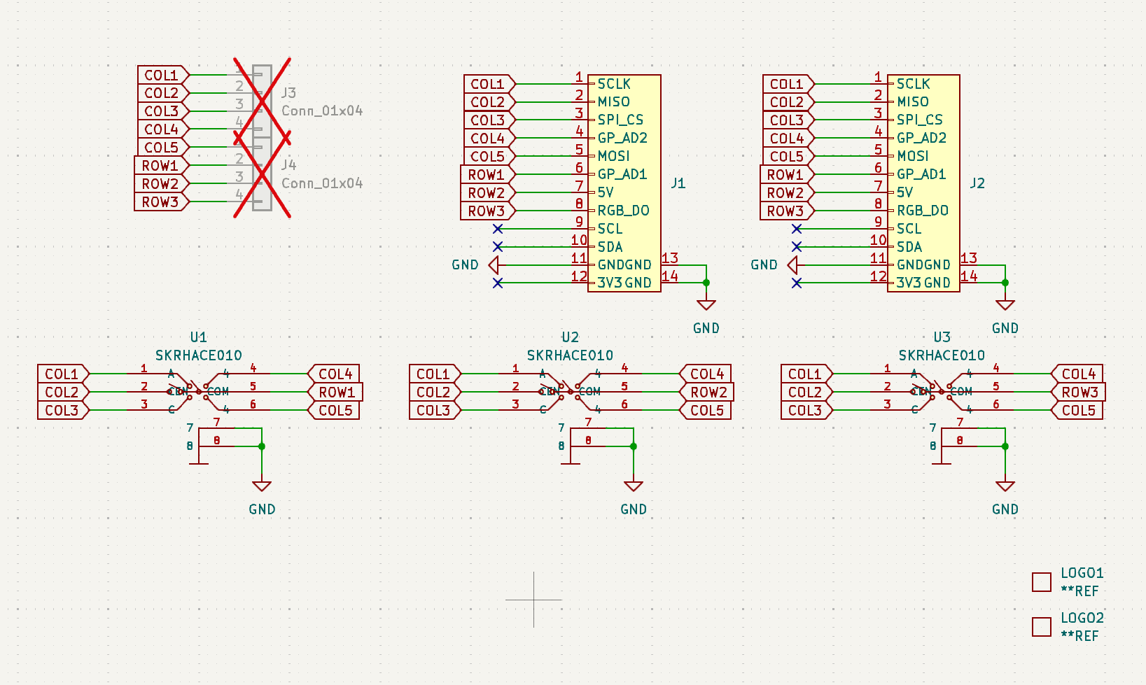
It is built around the SKRHACE010. Its parts include 4 connectors and 3 ICs.
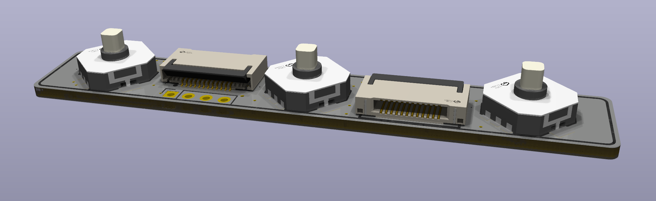
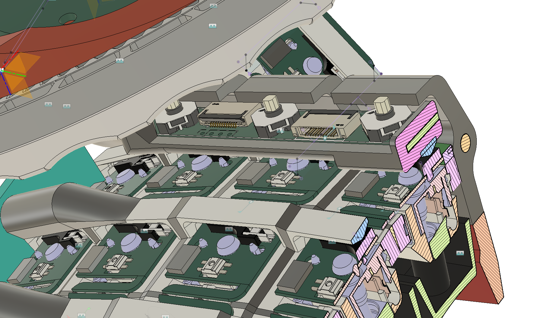
A single pcb for mk21 paddles, typewriter-esque. The 5way switches offer a really nice-feeling switch actuation - in future I'd look for a single-action button.
| Designator | Footprint | Quantity | Value | LCSC Part # |
|---|---|---|---|---|
| J1, J2 | FPC-SMD_12P-P0.50_XUNPU_FPC-05FB-12PH20 | 2 | vik-module-connector | C2856829 |
| U1, U2, U3 | SW-SMD_SKRHACE010 | 3 | SKRHACE010 | C209766 |
| Qty | Value | Footprint | References |
|---|---|---|---|
| 3 | SKRHACE010 | kicad-libraries:SW-SMD_SKRHACE010 | U1, U2, U3 |
| 2 | Conn_01x04 | Connector_PinSocket_2.00mm:PinSocket_1x04_P2.00mm_Vertical | J3, J4 |
| 2 | vik-module-connector | kicad-libraries:FPC-SMD_12P-P0.50_XUNPU_FPC-05FB-12PH20 | J1, J2 |
| 1 | **REF | kicad-libraries:awesome-logo | LOGO1 |
| 1 | **REF | kicad-libraries:multi-paddle-pcb-qr-8mm | LOGO2 |


christrotter/paddle-dpad-pcb
Prototype pcb to mount ALPS SKRACE010 switches on the back of the thumbcluster.

gwaves/smart-keyboard
ESP32-S3 detachable USB macro keyboard: firmware, macOS configurator, protocol, and KiCad hardware prototype


FrameworkComputer/ExpansionCards
Reference designs and documentation to create Expansion Cards for the Framework Laptop
It measures 60 × 10 mm and has 2 copper layers, 1.2 mm thick.
9 parts, built around the SKRHACE010. The full list of its parts is on this page, with links to each part's symbol and footprint where PCBKit's library has them.
From the christrotter/multi-paddle-pcb repository on GitHub, at the commit this page was made from: the board is multi-paddle-pcb.kicad_pcb and its schematic multi-paddle-pcb.kicad_sch. PCBKit opens the board in the browser, with nothing to install.
Its repository publishes it under the MIT licence: you may reuse it on that licence's terms (keep the author's notice, and for a copyleft licence share your changes alike).