4 layers37.1 × 61.5 mm
MCLZ8 PCB
MicroCoreLabs/Projects
Ted Fried's MicroCore Labs Projects - FPGA CPU cores and emulators for the 8088, 8086, 8051, 6502, 68000, Z80, Risc-V, and also Typewriter and EPROM Emulator projects.
6 parts534

 chibiosya/daedalus-core-pdn
Supplied KiCad 8 board asset for the Daedalus core PDN exercise (CC0-1.0)
Daedalus core pdn is an open-source printed circuit board by chibiosya, from the chibiosya/daedalus-core-pdn repository on GitHub, published under the CC0-1.0 licence. It is a 4-layer board of 60 × 40 mm with 6 parts on 2 nets, routed with 49 tracks and 57 vias.
Supplied KiCad 8 board asset for the Daedalus core power-delivery-network (PDN) exercise: a 60 x 40 mm, 4-layer board carrying a 225-ball SoC (U1) with its core-supply fanout, a VRM output (U2), a GND plane, a VDD_CORE plane, four mounting holes and a set of named keepout areas. It is meant to be designed onto: you add decoupling capacitors, their vias and tracks; everything that is already here is a supplied item and must not be moved or changed.
| File | Purpose |
|---|---|
daedalus_core_pdn.kicad_pcb | The board (KiCad 8 format, version 20240108, all footprints embedded, zones filled) |
daedalus_core_pdn.kicad_pro | Project: numeric design-rule constraints and the Default net class |
daedalus_core_pdn.kicad_dru | Custom rules: no via-in-pad, the keepout rules, the mounting-hole copper keepout |
supplied_items.json | UUID + geometry of every supplied item (footprints, tracks, vias, zones, rule areas, edge cuts, groups) and the U1 ball map |
tools/ | Reproducible generator / zone filler / verifier / build script |
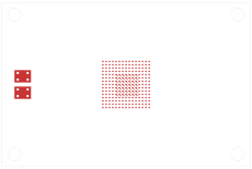
images/ | SVG renders of F.Cu, B.Cu, In1.Cu and In2.Cu |
Keep the three daedalus_core_pdn.* files together. kicad-cli pcb drc loads the .kicad_pro
and .kicad_dru that sit next to the board; without them KiCad falls back to its defaults
(0.2 mm net-class clearance) and the supplied BGA fanout no longer passes DRC.
kicad-cli)kicad-cli pcb drc --severity-error --exit-code-violations daedalus_core_pdn.kicad_pcb -> exit 0, 0 violations, 0 unconnected
kicad-cli pcb drc --severity-warning --exit-code-violations daedalus_core_pdn.kicad_pcb -> exit 0, 0 violations (no warnings remain)The keepout rules were proven to fire with a negative-test board (tools/generate_board.py --negative-test): a C_0402 capacitor placed inside KO_BGA_TOP, a via inside KO_VRM, a track inside
KO_DDR_CHANNEL on B.Cu, a via inside KO_MH1 and a via inside a non-U2 SMD pad are each reported as
an error by the corresponding rule (ko_bga_top, ko_vrm, ko_ddr_channel, ko_mh1 +
mounting_hole_copper_keepout, no_via_in_pad), and a via centred between two adjacent U1 balls
(A1/A2, at 94.8, 74.4) fails on clearance to the ball pads while ko_bga_top fires only on the
capacitor, not on any via. A positive-test board (--positive-test) with one via at an outer-ring
interstitial position of the ball grid (A1 + (0.4, 0.4) = 94.8, 74.8, inside KO_BGA_TOP but
outside the core 7x7 field) passes DRC with 0 violations. tools/build.sh re-runs both tests
every build.
| # | Layer | Type | Thickness | Note |
|---|---|---|---|---|
| 1 | F.Cu | copper | 0.035 mm | signal, components |
| dielectric 1 | prepreg FR4 | 0.200 mm | ||
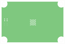
| 2 | In1.Cu | copper | 0.035 mm | GND plane |
| dielectric 2 | core FR4 | 1.000 mm | ||
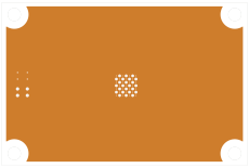
| 3 | In2.Cu | copper | 0.035 mm | VDD_CORE plane |
| dielectric 3 | prepreg FR4 | 0.200 mm | ||
| 4 | B.Cu | copper | 0.035 mm | signal |
Solder-mask layers are entered with 0 thickness so the stackup total shown by KiCad equals the specified 1.54 mm.
GND (net 1) and VDD_CORE (net 2). There are no other nets; 176 of the U1 balls are
intentionally unconnected.mounting_hole_copper_keepout
below and the KO_MH rule areas.BGA-225_15x15_0.8mm, reference U1, centre (100.000, 80.000), rotation 0, body
12 x 12 mm, courtyard (F.CrtYd) 13 x 13 mm centred on U1.VDD_CORE where (i + j) is even (25 balls), GND where odd (24 balls), i,j = 0..6 inside the
block. Every other ball has no net.Ball map (V = VDD_CORE, G = GND, . = no net):
| row \ col | 1 | 2 | 3 | 4 | 5 | 6 | 7 | 8 | 9 | 10 | 11 | 12 | 13 | 14 | 15 |
|---|---|---|---|---|---|---|---|---|---|---|---|---|---|---|---|
| A | . | . | . | . | . | . | . | . | . | . | . | . | . | . | . |
| B | . | . | . | . | . | . | . | . | . | . | . | . | . | . | . |
| C | . | . | . | . | . | . | . | . | . | . | . | . | . | . | . |
| D | . | . | . | . | . | . | . | . | . | . | . | . | . | . | . |
| E | . | . | . | . | V | G | V | G | V | G | V | . | . | . | . |
| F | . | . | . | . | G | V | G | V | G | V | G | . | . | . | . |
| G | . | . | . | . | V | G | V | G | V | G | V | . | . | . | . |
| H | . | . | . | . | G | V | G | V | G | V | G | . | . | . | . |
| J | . | . | . | . | V | G | V | G | V | G | V | . | . | . | . |
| K | . | . | . | . | G | V | G | V | G | V | G | . | . | . | . |
| L | . | . | . | . | V | G | V | G | V | G | V | . | . | . | . |
| M | . | . | . | . | . | . | . | . | . | . | . | . | . | . | . |
| N | . | . | . | . | . | . | . | . | . | . | . | . | . | . | . |
| P | . | . | . | . | . | . | . | . | . | . | . | . | . | . | . |
| R | . | . | . | . | . | . | . | . | . | . | . | . | . | . | . |
U1_FANOUT.VRM_OUT, reference U2, centre (75.000, 80.000), courtyard 6 x 8 mm centred on U2.VDD_CORE: SMD rectangle 4.0 x 3.0 mm on F.Cu centred at (75.0, 78.0).GND: SMD rectangle 4.0 x 3.0 mm on F.Cu centred at (75.0, 82.0).U2_VIAS.| Use | Diameter | Drill | Annular ring |
|---|---|---|---|
| U1 dog-bone vias (49) | 0.450 mm | 0.200 mm | 0.125 mm |
| U2 output vias (8) | 0.600 mm | 0.300 mm | 0.150 mm |
Default net class via (for anything you add) | 0.450 mm | 0.200 mm | 0.125 mm |
The keepouts are named rule areas with no keepout flags of their own; the enforcement lives in
daedalus_core_pdn.kicad_dru so that supplied items can be exempted while anything added later
is checked. Inside each area footprints, vias and tracks are forbidden on the listed layers, with
one exception: KO_BGA_TOP forbids footprints and tracks only. Vias are allowed under the BGA,
subject to the normal rules against the ball pads (0.100 mm clearance, 0.250 mm hole-to-copper
clearance, no_via_in_pad). In practice that means the interstitial positions of the ball grid
(ball centre + (±0.4, ±0.4) mm), where the supplied dog-bone vias already sit with 0.141 mm
clearance; a via centred between two adjacent balls overlaps their pads and fails.
| Name | Layers | Forbids | Shape | Coordinates (mm) | Exempt supplied items |
|---|---|---|---|---|---|
| KO_BGA_TOP | F.Cu | footprints, tracks (vias allowed) | 14 x 14 mm square | x 93..107, y 73..87 (centre 100,80) | U1, group U1_FANOUT |
| KO_DDR_CHANNEL | F.Cu, B.Cu | footprints, vias, tracks | rectangle | x 108..130, y 64..96 | none |
| KO_CONNECTOR | F.Cu, B.Cu | footprints, vias, tracks | rectangle | x 70..90, y 60..70 | H1 |
| KO_VRM | F.Cu, B.Cu | footprints, vias, tracks | rectangle | x 70..81, y 74..86 | U2, group U2_VIAS |
| KO_MH1 | all copper | footprints, vias, tracks | circle r 3.5 mm (72-gon) | centre (73,63) | H1 |
| KO_MH2 | all copper | footprints, vias, tracks | circle r 3.5 mm (72-gon) | centre (127,63) | H2 |
| KO_MH3 | all copper | footprints, vias, tracks | circle r 3.5 mm (72-gon) | centre (73,97) | H3 |
| KO_MH4 | all copper | footprints, vias, tracks | circle r 3.5 mm (72-gon) | centre (127,97) | H4 |
Rule areas in KiCad are polygons, so each circle is a 72-sided polygon with its vertices on the 3.5 mm radius. A footprint counts as inside an area when its courtyard intersects the area (KiCad semantics), so give your capacitors a courtyard.
Numeric constraints (.kicad_pro, Board Setup > Constraints):
| Constraint | Value |
|---|---|
| Minimum clearance | 0.100 mm |
| Minimum track width | 0.150 mm |
| Minimum via diameter | 0.450 mm |
| Minimum via drill (through hole) | 0.200 mm |
| Minimum annular ring | 0.125 mm |
| Hole-to-hole clearance | 0.250 mm |
| Copper-to-hole clearance | 0.250 mm (KiCad default) |
| Copper-to-edge clearance | 0.500 mm |
| Courtyard overlap | error |
| Silkscreen / solder-mask rules | KiCad defaults |
Net class Default: clearance 0.100 mm, track width 0.200 mm, via 0.450 / 0.200 mm. (The clearance
is set equal to the minimum clearance because KiCad's default of 0.2 mm would fail the specified
BGA fanout, whose via-to-neighbouring-ball gap is 0.141 mm.)
Custom rules (.kicad_dru, KiCad 8 syntax):
(rule no_via_in_pad
	(condition "A.Type == 'Via' && B.Type == 'Pad' && B.Pad_Type == 'SMD' && !B.memberOfFootprint('U2')")
	(constraint physical_clearance (min 0.1mm)))
No via may touch or come within 0.1 mm of any SMD pad, regardless of net. U2's pads are supplied with vias inside them and are the only exemption.
(rule ko_bga_top
	(layer "F.Cu")
	(condition "A.intersectsArea('KO_BGA_TOP') && !A.memberOfFootprint('U1') && !(A.Type == 'Footprint' && A.Reference == 'U1') && !A.memberOfGroup('U1_FANOUT')")
	(constraint disallow footprint track))
One such rule per keepout (ko_bga_top, ko_ddr_channel, ko_connector, ko_vrm, ko_mh1..4),
each restricted to the area's layers ((layer outer) for F.Cu + B.Cu, no layer clause for
all-copper) and exempting only the supplied items listed in the table above. All of them except
ko_bga_top use (constraint disallow footprint via track); ko_bga_top omits via, so vias
under the BGA are governed by the clearance, hole-to-copper and no_via_in_pad rules only.
(rule mounting_hole_copper_keepout
	(condition "B.Pad_Type == 'NPTH, mechanical'")
	(constraint hole_clearance (min 1.9mm)))
Hole edge (radius 1.6 mm) + 1.9 mm = the 3.5 mm copper-free radius around each mounting hole. This is honoured by the zone filler (the planes already have the cut-outs) and by DRC for any copper you add.
Capacitor via proximity is checked by the grader, not by DRC.
From the official KiCad library Capacitor_SMD: C_0201_0603Metric, C_0402_1005Metric,
C_0603_1608Metric, C_0805_2012Metric, C_1210_3225Metric. The Value field must be exactly
one of 0.1uF 0.22uF 0.47uF 1.0uF 2.2uF 4.7uF 10uF 22uF 47uF 100uF (as allowed per package in the
brief).
supplied_items.json lists every supplied object with its UUID and geometry: 6 footprints (U1, U2,
H1..H4), 49 tracks, 57 vias, 2 planes, 8 rule areas, the Edge.Cuts rectangle and the 2 groups, plus
the U1 ball map. UUIDs are deterministic (UUID v5 of the item name) so a regenerated board has the
same IDs. python3 tools/verify_board.py daedalus_core_pdn.kicad_pcb supplied_items.json checks
that all of them are still present and that the geometry matches this document.
KICAD_APP=/Applications/KiCad/KiCad.app tools/build.shtools/generate_board.py (stdlib Python, no KiCad needed) writes the three KiCad files and
supplied_items.json from the numbers above; tools/finalize_board.py (KiCad's bundled python,
pcbnew) fills the zones and re-saves in canonical KiCad 8 format; tools/build.sh then runs
DRC at error and warning severity, the negative and positive keepout tests, the verifier and the
SVG exports.
Built and validated with KiCad 8.0.9 on macOS.
| F.Cu | B.Cu |
|---|---|
 |  |
| In1.Cu (GND plane) | In2.Cu (VDD_CORE plane) |
|---|---|
 |  |
intersectsArea (any overlap is a violation), the same test KiCad uses for its
own rule-area keepouts.ko_bga_top no longer disallows vias (disallow footprint track
instead of disallow footprint via track). The keepout was meant to keep components and tracks
off the top side under the BGA, not to forbid through vias at the interstitial positions of the
ball grid, which the supplied dog-bones already use. Vias under the BGA are governed by the
normal clearance, hole-to-copper and no_via_in_pad rules. Negative test extended (via between
two balls must fail on clearance) and a positive test added (interstitial via must pass). Board,
project file and supplied_items.json are unchanged.CC0 1.0 Universal (public domain dedication), see LICENSE.
| Qty | Value | Footprint | References |
|---|---|---|---|
| 4 | MountingHole_3.2mm | MountingHole_3.2mm | H1, H2, H3, H4 |
| 1 | SoC | BGA-225_15x15_0.8mm | U1 |
| 1 | VRM_OUT | VRM_OUT | U2 |
MicroCoreLabs/Projects
Ted Fried's MicroCore Labs Projects - FPGA CPU cores and emulators for the 8088, 8086, 8051, 6502, 68000, Z80, Risc-V, and also Typewriter and EPROM Emulator projects.


lucanastasio/PCIexpress-KiCad
PCI express libraries and templates for KiCad

BerkeleyHCI/PolymorphicBlocks
A Python-based hardware description language for PCBs for higher-level (block-diagram / system-architecture level) PCB design through libraries of directly reusable subcircuit generators.

buganini/Kikakuka
Kikakuka — KiCad Workspace, Panelization, Build Variants, Differ & FreeCAD PCB Bending and Assembly

matthuszagh/fmcw
6GHz frequency-modulated continuous-wave radar with real-time range detection

google/myelin-acorn-electron-hardware
Phillip Pearson's retro hardware projects for the Acorn Electron
It measures 60 × 40 mm and has 4 copper layers, 1.54 mm thick.
6 parts. The full list of its parts is on this page, with links to each part's symbol and footprint where PCBKit's library has them.
From the chibiosya/daedalus-core-pdn repository on GitHub, at the commit this page was made from: the board is daedalus_core_pdn.kicad_pcb. PCBKit opens the board in the browser, with nothing to install.
Its repository publishes it under the CC0-1.0 licence: you may reuse it on that licence's terms (keep the author's notice, and for a copyleft licence share your changes alike).