
2 layers30.4 × 12.7 mm

 cfrankb/pcb_ch552_devboard1
CH552 Devboard with ON/OFF switch, BOOT and RESET buttons. Indicator lights and lots of pins.
Pcb ch552 devboard is an open-source printed circuit board by cfrankb, from the cfrankb/pcb_ch552_devboard repository on GitHub. It is a 2-layer board of 50 × 50 mm with 33 parts on 31 nets, routed with 127 tracks and 3 vias.
It is built around the CH552G. Its parts include 9 connectors, 8 resistors, 6 diodes, 3 capacitors and 2 switches. It belongs with the microcontroller boards boards and the 8051 (CH55x, STC, AT89) boards of this library.
This is a pcb design for a CH552 DEVBOARD. The board is intended to aid in the development of firmware/prototype for the CH552 and CH554 microcontrollers.
The Power Switch (Workflow Optimization): The CH552 enters ISP (programming) mode based on power-on state with a specific pin held. Constantly pulling a USB cable wears out the connector and is inefficient. Your switch demonstrates mechanical sympathy and an understanding of the iterative development cycle.
The "Ground Forest" (Signal Integrity): Adding 12x GND pins isn't overkill—it's professional. It allows you to clip a logic analyzer, an oscilloscope probe, and multiple peripherals simultaneously without creating a "rat's nest" of wires sharing a single pin.
The "Ground Forest" (Signal Integrity): Having 4 LEDs dedicated to the MCU pins allows for immediate visual confirmation of state machines or "heartbeat" signals without needing to wire up external breadboard components.
https://github.com/cfrankb/ch552_drivers/
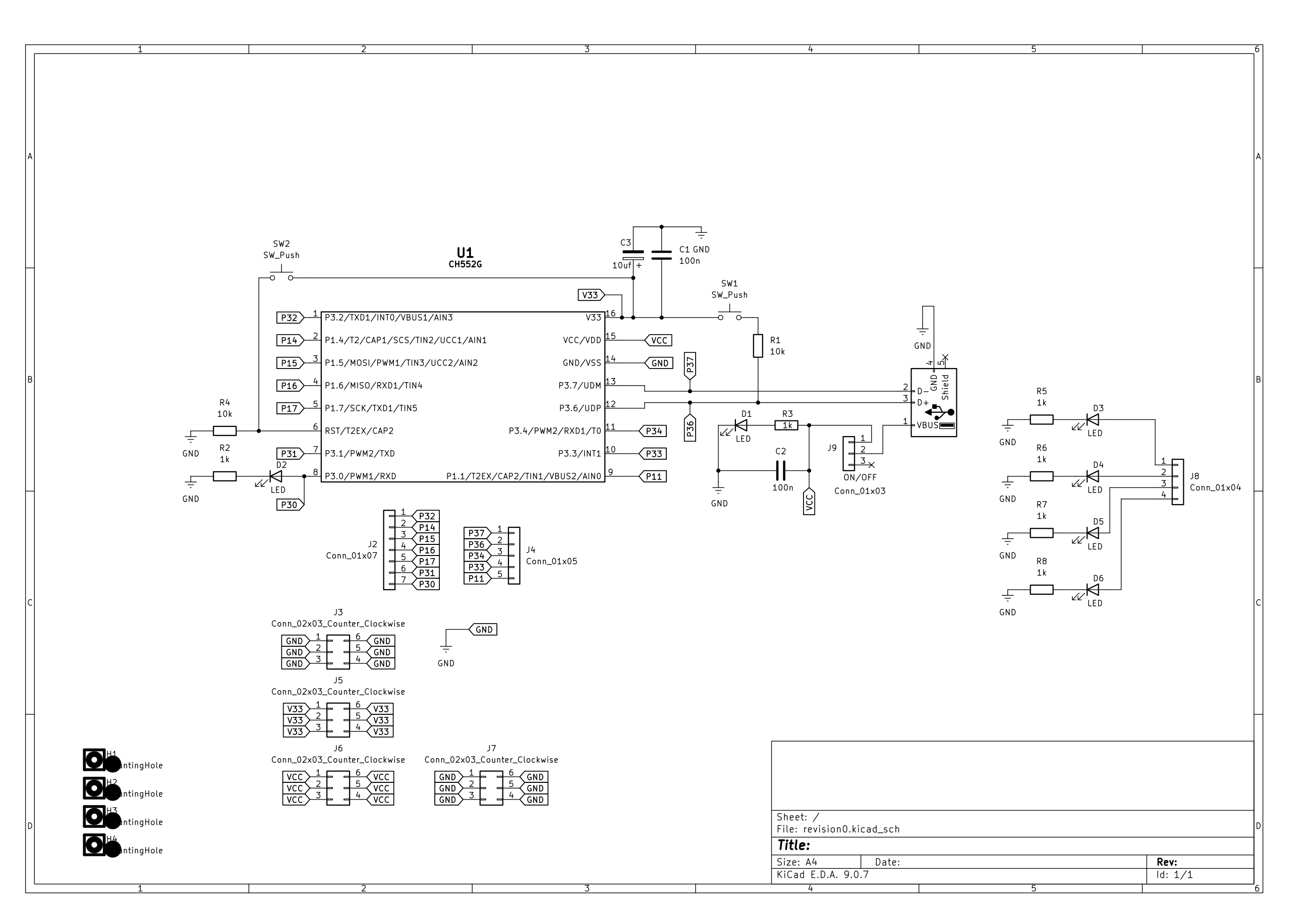
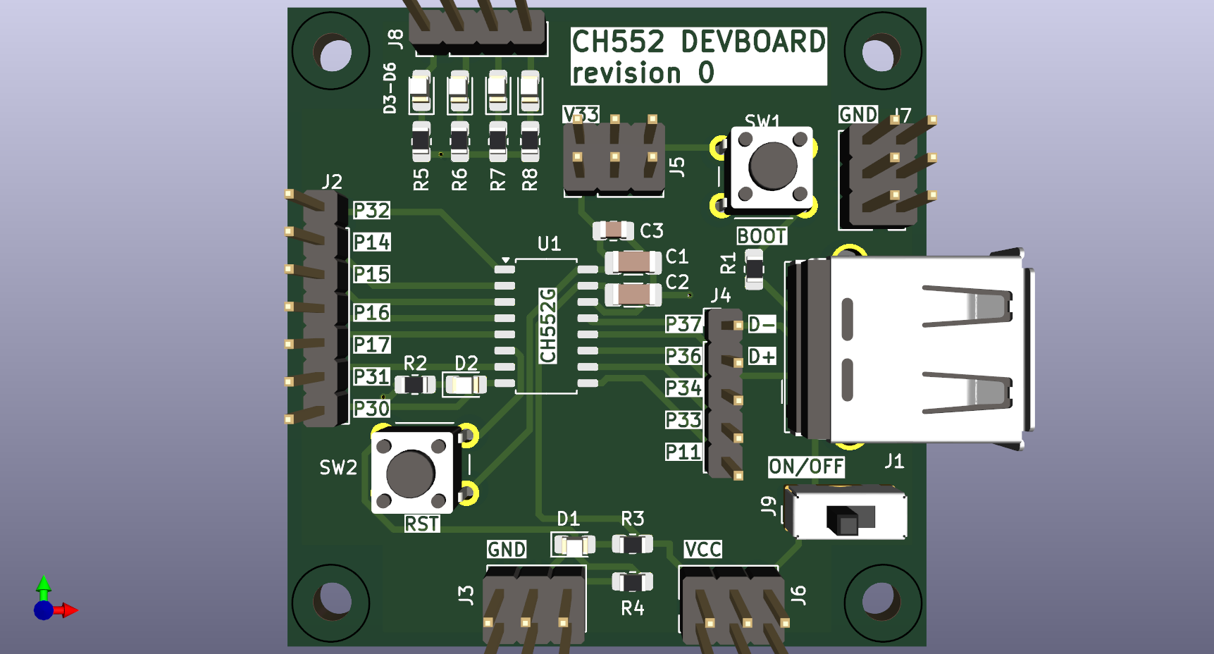
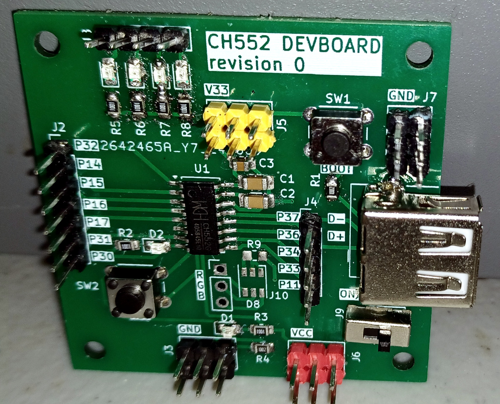
| Part # | REF# | Package | |
|---|---|---|---|
| 1x | 10u C | C3 | 0805 |
| 2x | 100n C | C1, C2 | 1206 |
| 2x | 10k Resistor | R1, R4 | 0805 |
| 6x | 1k Resistor | R2, R3, R5, R6, R7, R8 | 0805 |
| 1x | Green Led | D1 | 0805 |
| 5x | Leds | D2, D3, D4, D5, D6 | 0805 |
| 1x | CH552G/CH554G | U1 | SOP16 |
| 2x | button | SW1, SW2 | 6x6x4.3mm DIP |
| 1x | USB Connector | J1 | USB 2.0 Female DIP |
| 1x | 1x07 | J2 | 2.54mm pins DIP |
| 1x | 2x03 | J3, J5, J6, J7 | 2.54mm pins DIP |
| 1x | 1x05 | J4 | 2.54mm pins DIP |
| 1x | 1x04 | J8 | 2.54mm pins DIP |
| 1x | 1x03 | J9 | SS12D00 DIP * |
* You can also use a 2.54mm pin header with a jumper cap.
| Qty | Value | Footprint | References |
|---|---|---|---|
| 6 | 1k | Resistor_SMD:R_0805_2012Metric_Pad1.20x1.40mm_HandSolder | R2, R3, R5, R6, R7, R8 |
| 6 | LED | LED_SMD:LED_0805_2012Metric_Pad1.15x1.40mm_HandSolder | D1, D2, D3, D4, D5, D6 |
| 4 | Conn_02x03_Counter_Clockwise | Connector_PinHeader_2.54mm:PinHeader_2x03_P2.54mm_Vertical | J3, J5, J6, J7 |
| 4 | MountingHole | MountingHole:MountingHole_3mm | H1, H2, H3, H4 |
| 2 | 100n | Capacitor_SMD:C_1206_3216Metric_Pad1.33x1.80mm_HandSolder | C1, C2 |
| 2 | 10k | Resistor_SMD:R_0805_2012Metric_Pad1.20x1.40mm_HandSolder | R1, R4 |
| 2 | SW_Push | Button_Switch_THT:SW_PUSH_6mm_H4.3mm | SW1, SW2 |
| 1 | 10uf | Capacitor_SMD:C_0805_2012Metric_Pad1.18x1.45mm_HandSolder | C3 |
| 1 | CH552G | Package_SO:SOP-16_4.55x10.3mm_P1.27mm | U1 |
| 1 | Conn_01x03 | Connector_PinHeader_2.54mm:PinHeader_1x03_P2.54mm_Vertical | J9 |
| 1 | Conn_01x04 | Connector_PinHeader_2.54mm:PinHeader_1x04_P2.54mm_Vertical | J8 |
| 1 | Conn_01x05 | Connector_PinHeader_2.54mm:PinHeader_1x05_P2.54mm_Vertical | J4 |
| 1 | Conn_01x07 | Connector_PinHeader_2.54mm:PinHeader_1x07_P2.54mm_Vertical | J2 |
| 1 | USB1 | usb:USB_A_Molex_67643_Horizontal | J1 |
It measures 50 × 50 mm and has 2 copper layers, 1.6 mm thick.
33 parts, built around the CH552G. The full list of its parts is on this page, with links to each part's symbol and footprint where PCBKit's library has them.
From the cfrankb/pcb_ch552_devboard repository on GitHub, at the commit this page was made from: the board is revision0/revision0.kicad_pcb and its schematic revision0/revision0.kicad_sch. PCBKit opens the board in the browser, with nothing to install.
Its repository states no licence, so its author keeps all rights: ask cfrankb before reusing the design.


milar111/L.I.P.S.
OpenSource Affordable SipAndPuff device: Linear Interface for Paralysis Support


gowenrw/BSidesDFW_2019_Badge
This is where all the files for the BSidesDFW 2019 Badge will be stored. This includes code and art and cab and fab files. All the things.
