2 layers37 × 19 mm
Passive rpi hub75-adapter
hzeller/rpi-rgb-led-matrix
Controlling up to three chains of 64x64, 32x32, 16x32 or similar RGB LED displays using Raspberry Pi GPIO
2 parts4.4kGPL-2.0

 cepawiel/DC_G2_TP_FFC4
Dreamcast G2 Test Points to FFC Connector
G2 Testpoints FFC is an open-source printed circuit board by cepawiel, from the cepawiel/DC_G2_TP_FFC repository on GitHub, published under the MIT licence. It is a 2-layer board of 35.1 × 57.2 mm with 2 parts on 37 nets, routed with 235 tracks and 33 vias.
Dreamcast G2 Test Points to FFC Connector. This was designed for a VA1 console, have yet to test on VA0 or VA2.
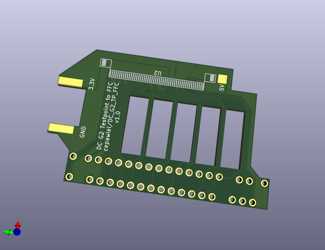
| Part | Quantity | Description | URL |
|---|---|---|---|
| THD0515-50CL-SN | 1 | 50Pin 0.5MM FFC Bottom Contact Connector | https://www.lcsc.com/product-detail/FFC-FPC-Connectors_THD-THD0515-50CL-SN_C283159.html |
| JS05B-50P-150-4-8 | 1 | 50Pin 0.5MM FFC Opposite Side 15CM | https://www.lcsc.com/product-detail/FFC-FPC-Connect-Cables_JUSHUO-JS05B-50P-150-4-8_C2857761.html |
Tested working, ordered from JLCPCB. I chose 1.6mm thickness, but I might try thiner next time to make it easier to solder to the test points
| Qty | Value | Footprint | References |
|---|---|---|---|
| 1 | G2_FFC | DreamcastCommon:G2_Testpoints | U1 |
| 1 | G2_FFC | DreamcastCommon:G2_FFC | U2 |
hzeller/rpi-rgb-led-matrix
Controlling up to three chains of 64x64, 32x32, 16x32 or similar RGB LED displays using Raspberry Pi GPIO


adamws/kicad-kbplacer
KiCad plugin for automatic keyboard's key placement and routing

Luos-io/luos_engine
Open-source and real-time orchestrator for cyber-physical-systems, to easily design, test and deploy embedded applications and digital twins.

NVNTLabs/switch2-SDEX2M2
Micro SD Express to M.2 NVME Adapter for Nintendo Switch 2

BlueSCSI/BlueSCSI-v2
BlueSCSI v2/Ultra - an open source, open hardware, SCSI emulator using the Pi Pico PR2040 and Pico 2 RP2350

ohmtech-rdi/eurorack-blocks
Software to Hardware Prototyping for Eurorack using C++, Max/Gen~ or Faust

It measures 35.1 × 57.2 mm and has 2 copper layers, 1.6 mm thick.
2 parts. The full list of its parts is on this page, with links to each part's symbol and footprint where PCBKit's library has them.
From the cepawiel/DC_G2_TP_FFC repository on GitHub, at the commit this page was made from: the board is G2_Testpoints_FFC.kicad_pcb and its schematic G2_Testpoints_FFC.kicad_sch. PCBKit opens the board in the browser, with nothing to install.
Its repository publishes it under the MIT licence: you may reuse it on that licence's terms (keep the author's notice, and for a copyleft licence share your changes alike).