
2 layers75 × 25 mm
Kicad mic amp
Despairon/kicad_mic_amp
KiCad project of a microphone amplifier with Codec and USB support.
35 partsMIT

 ccostes/usbMic16
USB Audio Interface
UsbAudio is an open-source printed circuit board by ccostes, from the ccostes/usbMic repository on GitHub. It is a 2-layer board of 42.6 × 14.1 mm with 39 parts on 44 nets, routed with 207 tracks and 16 vias.
It is built around the MIC5365-3.0YD5-TR. Its parts include 17 capacitors, 8 resistors, 4 ICs, 3 connectors and 1 crystal. It belongs with the audio and music and interfaces and adapters boards of this library.
This is a DIY USB microphone interface designed for an electret condenser microphone. It has up to 60dB of amplification and 16-bit ADC. This is my first PCB design and this page is intended to document the design itself, as well as my learnings along the way.
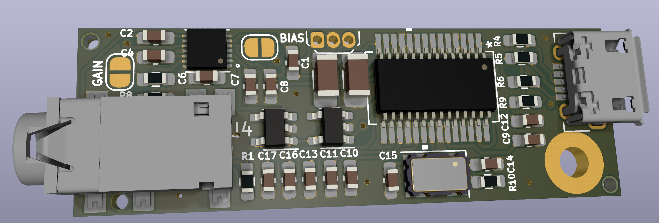
The project was created in KiCad 6
I haven't yet assembled or tested this board, will update when I do.
Mostly as an excuse to design and build a PCB - you can buy something to do the same thing for $10 on Amazon. I'm a software engineer professionally, but did my degree in Electrical and Computer engineering and always wanted to design a board from scratch to feel like a real engineer. 😆 Given that, I wouldn't take anything here as authoritative or good practice.
I did go a little over-the-top and design this with probably way more performance and features than necessary, but that's the fun of building things yourself!
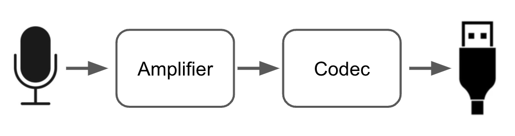
A USB Microphone interface sounds pretty complicated, but luckily there are off-the-shelf components that do everything we need so this design is quite simple with two main components: an amplifier (the little chip) and a USB codec (the big chip).
In case you're unfamiliar with electronic design, component manufacturers publish datasheets for each part that document the part itself but also typically show you an example circuit of how to use it (making it easier to use the parts sells more parts). That means putting together a design like this is mostly an exercise of reading the datasheet carefully and wiring things up the way they show you, but inevitably there are aspects that are left out/unclear/assume you know what you're doing, so things aren't quite that simple.
The first step in building a microphone interface is interfacing with a microphone, which is where the amplifier comes in. I chose the the MAX9814, primarily because it has built-in auto-gain-control (AGC) that will decrease the amplification to prevent the output from clipping loud input signals. It has three gain settings that go up to 60dB (which seems like a lot), and provides 2V bias for the microphone.
Electret microphones are actually a combo microphone/amplifier-transistor, and that transistor requires a bias voltage to operate. Check out this Open Music Labs page for a great explanation of electret microphones.
The amplifier microphone bias is 2V, but some high-performance microphones are rated for 3V, so I've added a 3V bias supply that is connected to the microphone by default, and a optional jumper for the amplifier-supplied 2V. If you want 2V, simply leave the 3V voltage regulator off (of cut the trace) and solder the jumper pads to connect the 2V bias.
Once the analog microphone signal is amplified we need to digitize it with an analog-to-digital converter (ADC) and send that over USB in a format that computers recognize. The ADC part isn't too complicated, but USB definitely is, so luckily TI makes the PCM2906 chip that does all of this (and more)!
This chip is rather expensive (currently over $12 on Digikey) and could be replaced by a standalone ADC and microcontroller to reduce cost, but doing so would increase design complexity and require custom software for the USB interface. I might try that as a follow-up design later, but want to keep things simple here which this chip does.
Now that we know the parts involved let's see how everything is wired up!
Again, most of this comes straight from the "Typical Application Circuit" examples in the datasheets (page 11 in the MAX datasheet and page 24 in the PCM2906), so I'll focus on the differences and challenges in going from those to this design.
The first thing to point out is that a lot of the wires in the schematic end with a label. All of the wires with the same labels are connected, and the label meanings are as follows:
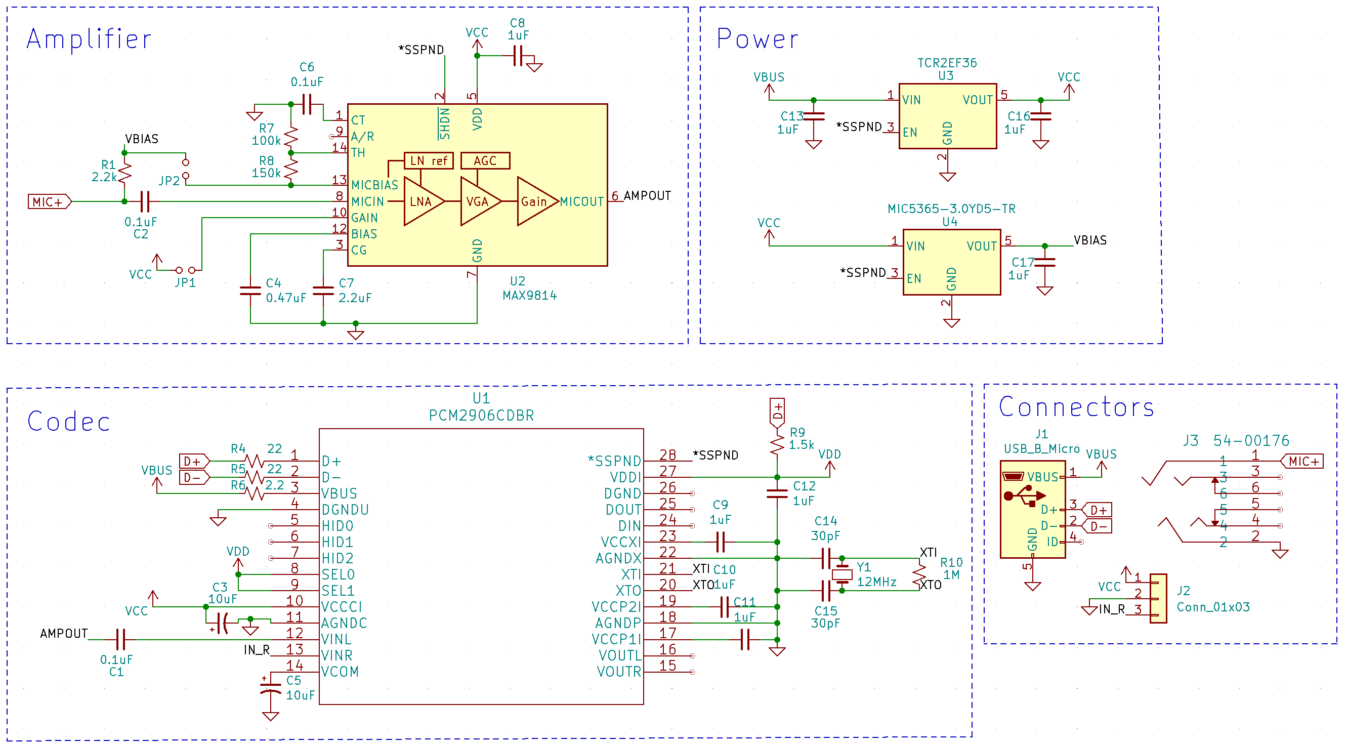
Starting with the simple stuff, in the bottom-right Connectors section you see the USB and Microphone connectors, along with an expansion header that brings out power, ground, and the right audio channel.
The top-right is the power-supply section, which takes the (noisy) 5V USB power supply and uses linear voltage regulators to produce 3.6V and 3V. Linear regulators are designed to produce the desired voltage regardless of the input voltage, and whatever difference is wasted as heat. They aren't usually the most efficient (though for a small difference between input and output voltage they can be), but they produce a very smooth output and reject noise that may be on the input supply which is important for the analog audio circuitry here.
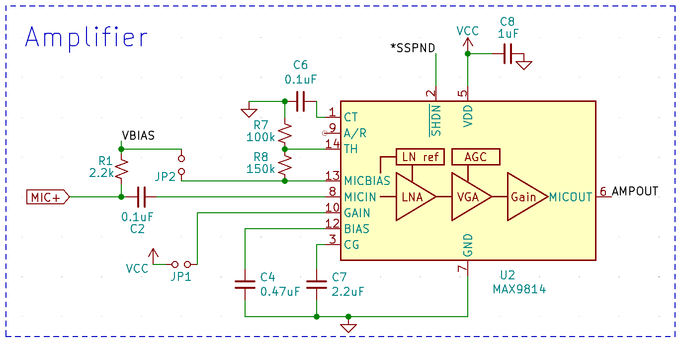 Starting at the top, the shutdown pin (
SHDN - the line over it means it is inverted logic so logic-low (0V) = shutdown) is wired to the *SSPND label (asterisk in place of the bar over the word, same meaning) rather than permanently connected to Vcc as in the datasheet. The *SSPND line allows the PCM to power the analog circuitry off when the microphone is not in use.
Moving to the left you can see the positive microphone input line (MIC+) is connected through R1 to both a label VBIAS as well as the MICBIAS pin of the amplifier through a jumper. As mentioned earlier, this board has both 3V and 2V mic bias supplies. The 3V is on VBIAS and is connected by default, and the 2V comes from the amplifier on MICBIAS and can be connected by the jumper, being sure to either leave off the 3V regulator or cut the trace. I'm not sure if anything bad would happen if they were both connected, but my guess is the amplifier wouldn't like its bias output to be connected to a higher voltage so I wouldn't recommend that.
Below the microphone lines you'll notice jumper JP1 between the GAIN pin and Vcc. The gain pin configures the maximum gain of the amplifier. Unconnected = 60dB, Ground = 50dB, and Vcc = 40dB. By default I have it unconnected to get the full 60dB range, but I thought that might be too much so added a solder jumper to allow that to be reduced to 40dB.
The amplifier output is on the right which goes to the AMPOUT label.
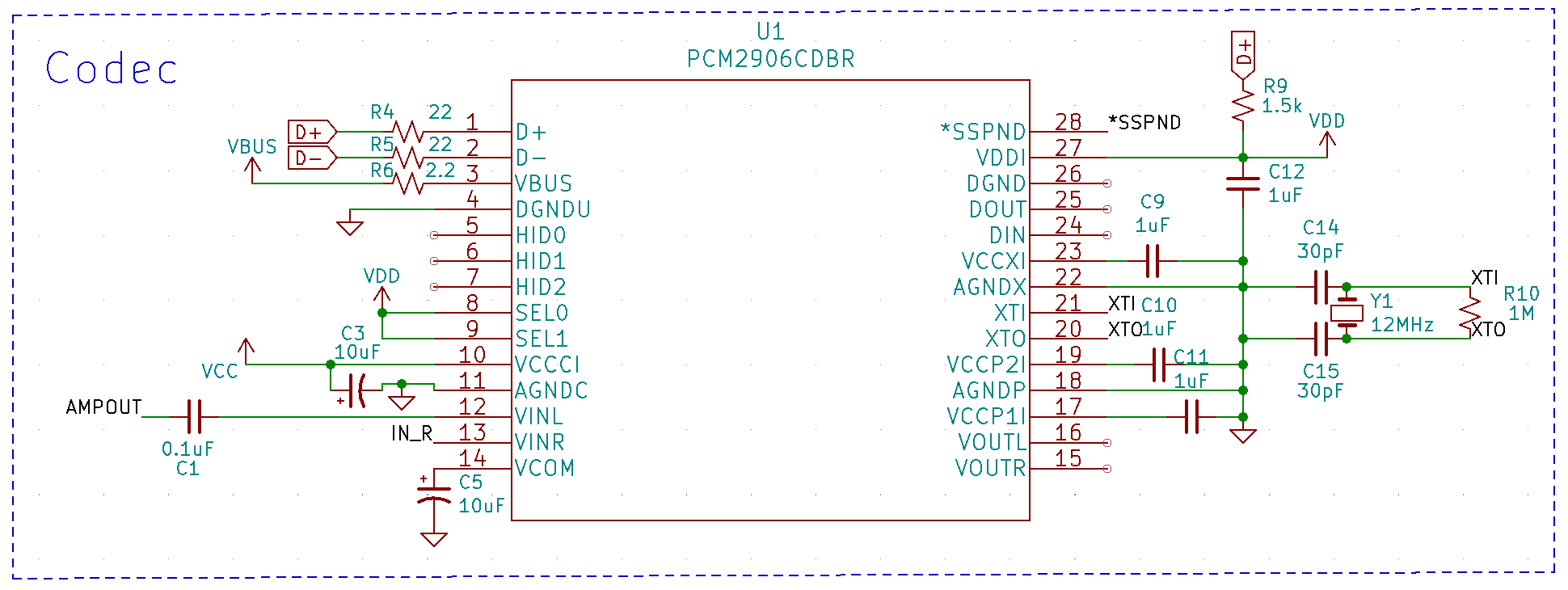
The main aspect of the codec I struggled with was how to connect the amplifier output - whether I could just connect them directly or if I needed some sort of matching circuitry. As you can see in the schematic, I only have a coupling capacitor between the two, which removes the bias voltage from the amplifier output and results in a 0V center voltage.
The MAX datasheet specifies that its output has a center-voltage of 1.23V which could be removed by placing a coupling capacitor in series. The PCM datasheet "Analog Input" section specified a center-voltage of Vcc/2, so I though that I needed to shift the output up by about 0.7V. Confusingly, the PCM datasheet example application ony showed coupling capacitors in front of the inputs - indicating 0V input bias.
I asked on reddit and a couple people pointed out that the block diagram of the Analog frontend shows that the input is internally biased, so needed a 0V center voltage and all I needed was the coupling capacitor as the schematic showed. I still think the Analog Input section should have specified 0V instead of Vcc/2 center voltage.
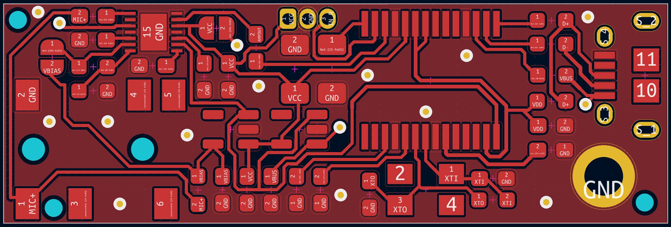
Full layout
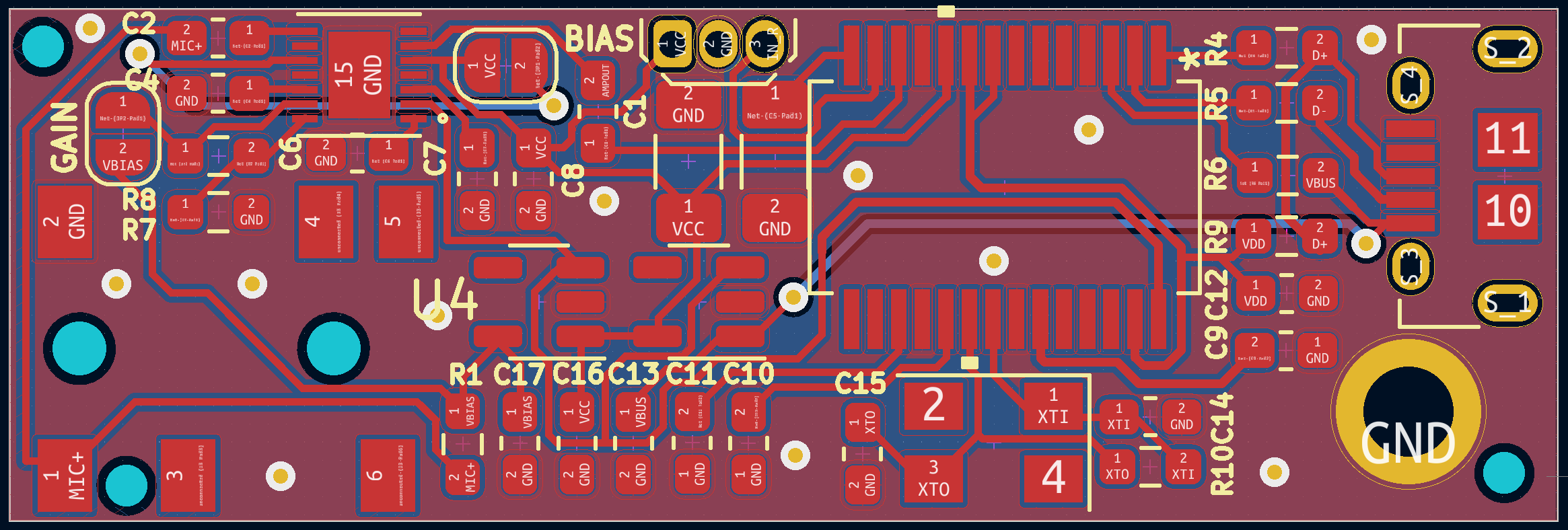 Front Copper
 Back Copper
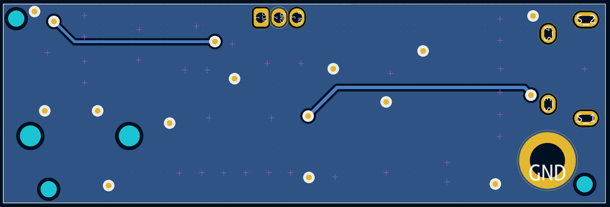
This layout went though a number of revisions and I learned a lot along the way. Making my own part footprints turned out to be really important. Some parts didn't have footprints available online, and even those that do should be inspected to make sure they actually match the datasheet.
I found the routing to be pretty difficult with KiCad (unsure if it's like this in all programs) because you can't 'move' the tra ces once you draw them, so rearranging things is quite time-consuming.
The board is almost single-sided; there were two power traces I put on the back side. I probably could have made a lot more use of the back side, but for some reason tried to minimize vias.
All parts other than the crystal are surface-mount (SMD), and I went with 0603 size resistors/capacitors. I've never constructed a PCB with components this small, so that will be another learning experience for sure. My plan is to hotplate reflow solder the surface-mount components.
| Qty | Value | Footprint | References |
|---|---|---|---|
| 8 | 1uF | Capacitor_SMD:C_0603_1608Metric_Pad1.08x0.95mm_HandSolder | C8, C9, C10, C11, C12, C13, C16, C17 |
| 3 | 0.1uF | Capacitor_SMD:C_0603_1608Metric_Pad1.08x0.95mm_HandSolder | C1, C2, C6 |
| 2 | 10uF | Capacitor_SMD:C_1206_3216Metric_Pad1.33x1.80mm_HandSolder | C3, C5 |
| 2 | 22 | Resistor_SMD:R_0603_1608Metric_Pad0.98x0.95mm_HandSolder | R4, R5 |
| 2 | 30pF | Capacitor_SMD:C_0603_1608Metric_Pad1.08x0.95mm_HandSolder | C14, C15 |
| 2 | Jumper_NO_Small | Jumper:SolderJumper-2_P1.3mm_Open_RoundedPad1.0x1.5mm | JP1, JP2 |
| 2 | MountingHole_2.1mm | MountingHole:MountingHole_2.1mm | ALIGN1, ALIGN2 |
| 1 | 0.47uF | Capacitor_SMD:C_0603_1608Metric_Pad1.08x0.95mm_HandSolder | C4 |
| 1 | 1.5k | Resistor_SMD:R_0603_1608Metric_Pad0.98x0.95mm_HandSolder | R9 |
| 1 | 100k | Resistor_SMD:R_0603_1608Metric_Pad0.98x0.95mm_HandSolder | R7 |
| 1 | 12MHz | Crystal:Crystal_SMD_5032-4Pin_5.0x3.2mm | Y1 |
| 1 | 150k | Resistor_SMD:R_0603_1608Metric_Pad0.98x0.95mm_HandSolder | R8 |
| 1 | 1M | Resistor_SMD:R_0603_1608Metric_Pad0.98x0.95mm_HandSolder | R10 |
| 1 | 2.2 | Resistor_SMD:R_0603_1608Metric_Pad0.98x0.95mm_HandSolder | R6 |
| 1 | 2.2k | Resistor_SMD:R_0603_1608Metric_Pad0.98x0.95mm_HandSolder | R1 |
| 1 | 2.2uF | Capacitor_SMD:C_0603_1608Metric_Pad1.08x0.95mm_HandSolder | C7 |
| 1 | 54-00176 | Connector:54-00177 | J3 |
| 1 | Conn_01x03 | Package_TO_SOT_THT:TO-92Flat | J2 |
| 1 | MAX9814 | max9814:max9814etd&plus_t | U2 |
| 1 | MIC5365-3.0YD5-TR | Package_TO_SOT_SMD:SOT-23-5 | U4 |
| 1 | PCM2906CDBR | pcm2906:PCM2906CDBR | U1 |
| 1 | TCR2EF36 | Package_TO_SOT_SMD:SOT-23-5 | U3 |
| 1 | USB_B_Micro | usb:10118194-0001LF | J1 |
The 37 most common of 39 parts.
It measures 42.6 × 14.1 mm and has 2 copper layers, 1.6 mm thick.
39 parts, built around the MIC5365-3.0YD5-TR. The full list of its parts is on this page, with links to each part's symbol and footprint where PCBKit's library has them.
From the ccostes/usbMic repository on GitHub, at the commit this page was made from: the board is usbAudio.kicad_pcb and its schematic usbAudio.kicad_sch. PCBKit opens the board in the browser, with nothing to install.
Its repository states no licence, so its author keeps all rights: ask ccostes before reusing the design.
Despairon/kicad_mic_amp
KiCad project of a microphone amplifier with Codec and USB support.


joeycastillo/Sensor-Watch
A board replacement for the classic Casio F-91W wristwatch

rusefi/rusefi
rusefi - GPL internal combustion engine control unit

hackclub/OnBoard
💡 Join 1,000 teenagers and make your first PCB with a $100 grant!

ataradov/usb-sniffer-lite
A simple USB sniffer based on Raspberry Pi RP2040

windowsair/wireless-esp8266-dap
CMSIS-DAP compatible wireless debugger for ESP8266/ESP32/ESP32C3/ESP32S3. Optional 40MHz SPI acceleration, etc. 适配多种ESP芯片的无线调试器
