2 layers37 × 19 mm
Passive rpi hub75-adapter
hzeller/rpi-rgb-led-matrix
Controlling up to three chains of 64x64, 32x32, 16x32 or similar RGB LED displays using Raspberry Pi GPIO
2 parts4.4kGPL-2.0
 BYU-ELC/PcbDesign2
Cam processing, Design rules, and common parts library for the ELC! Check back for updates.
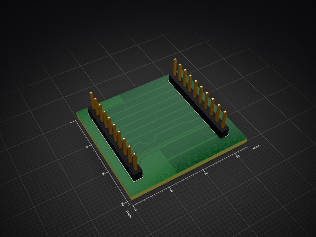
Design Rules Project is an open-source printed circuit board by BYU-ELC, from the BYU-ELC/PcbDesign repository on GitHub, published under the MIT licence. It is a 2-layer board of 34 × 31 mm with 2 parts on 10 nets, routed with 29 tracks and 0 vias.
Contains the following configuration files for the Brigham Young University Electrical and Computer Engineering Shop:
It is easiest to use this repository by using git, which on Windows has to be installed. Linux and Mac usually come with git installed. You can find out by opening a terminal (or PowerShell for Windows) and typing git version. If it is not installed, download it. If using a computer without administrative privileges (a school computer), download the Portable or "thumbdrive edition".
git version. If an error occurs, follow the instructions in the above paragraph to download git.cd commandgit clone https://github.com/BYU-ELC/PcbDesign byuPCBEvery once in a while, navigate to the directory chossen for download and execute git pull. This will keep your version of the file up to date.
This method is easier, but you will have to do it every time you want to submit a board for production. Using Git is highly recommended, but this option is included for completeness.
(Below this line is eagle specific.)
Remember, the file will have to be downloaded new each time it is used so that all updates will be available.
Below are links to JLC PCB's CAM and Design rule files because they are hard to find on the website.
CAM files: use jlcpcb_2_layer_v9.cam for most jobs
DRC files: use design_rules/jlcpcb-2layers.dru
| Qty | Value | Footprint | References |
|---|---|---|---|
| 1 | 1mm diameter | Connector_PinHeader_2.54mm:PinHeader_1x10_P2.54mm_Vertical | J2 |
| 1 | 2.54mm spaced headers | Connector_PinHeader_2.54mm:PinHeader_1x10_P2.54mm_Vertical | J1 |
hzeller/rpi-rgb-led-matrix
Controlling up to three chains of 64x64, 32x32, 16x32 or similar RGB LED displays using Raspberry Pi GPIO


adamws/kicad-kbplacer
KiCad plugin for automatic keyboard's key placement and routing

Luos-io/luos_engine
Open-source and real-time orchestrator for cyber-physical-systems, to easily design, test and deploy embedded applications and digital twins.

NVNTLabs/switch2-SDEX2M2
Micro SD Express to M.2 NVME Adapter for Nintendo Switch 2

BlueSCSI/BlueSCSI-v2
BlueSCSI v2/Ultra - an open source, open hardware, SCSI emulator using the Pi Pico PR2040 and Pico 2 RP2350

ohmtech-rdi/eurorack-blocks
Software to Hardware Prototyping for Eurorack using C++, Max/Gen~ or Faust

It measures 34 × 31 mm and has 2 copper layers, 1.6 mm thick.
2 parts. The full list of its parts is on this page, with links to each part's symbol and footprint where PCBKit's library has them.
From the BYU-ELC/PcbDesign repository on GitHub, at the commit this page was made from: the board is KiCAD/KiCad 7.0/Design Rules/Design_Rules_Project/Design_Rules_Project.kicad_pcb and its schematic KiCAD/KiCad 7.0/Design Rules/Design_Rules_Project/Design_Rules_Project.kicad_sch. PCBKit opens the board in the browser, with nothing to install.
Its repository publishes it under the MIT licence: you may reuse it on that licence's terms (keep the author's notice, and for a copyleft licence share your changes alike).