
2 layers49.6 × 78.3 mm
Odyssey
jotego/jtcores
FPGA cores compatible with multiple arcade game machines and KiCAD schematics of arcade games. Working on MiSTer FPGA/Analogue Pocket
24 parts346GPL-3.0

 bwack/TheFinalChessCard5
TheFinalChessCard for C64/C128, replicated using SprintLayout. Here are the sprint and gerber files.
Finalchesscard lvr draft1 is an open-source printed circuit board by bwack, from the bwack/TheFinalChessCard repository on GitHub. It is a 2-layer board of 148.9 × 58.1 mm with 40 parts on 106 nets, routed with 1,708 tracks and 116 vias.
It is built around the 74LS30PC. Its parts include 12 ICs, 10 capacitors, 6 diodes, 5 resistors and 1 switch.
TheFinalChessCard for C64/C128, replicated using SprintLayout. Here are the sprint and gerber files.
The scanned images are from the World of Jani blog article about this card. See also the forum64.de threads.
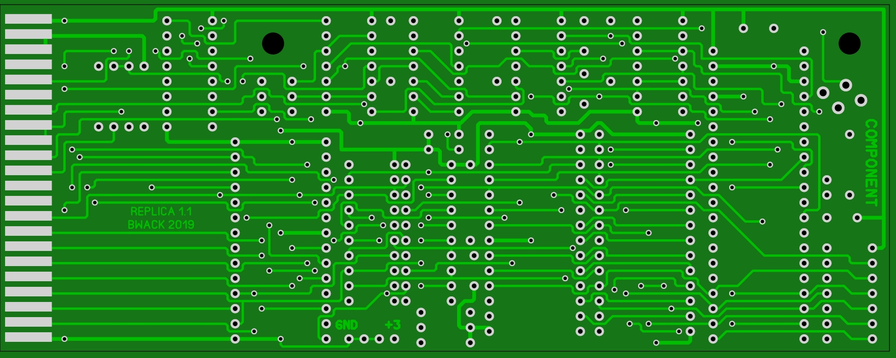
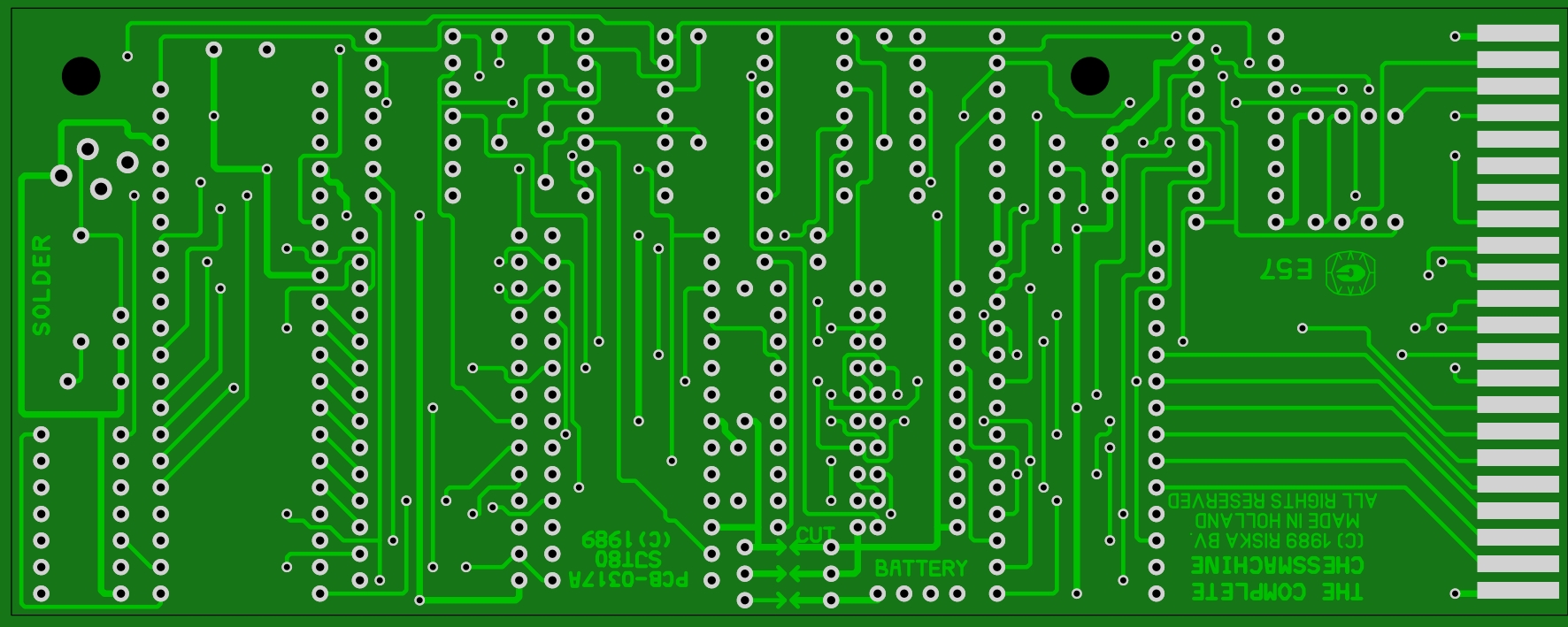
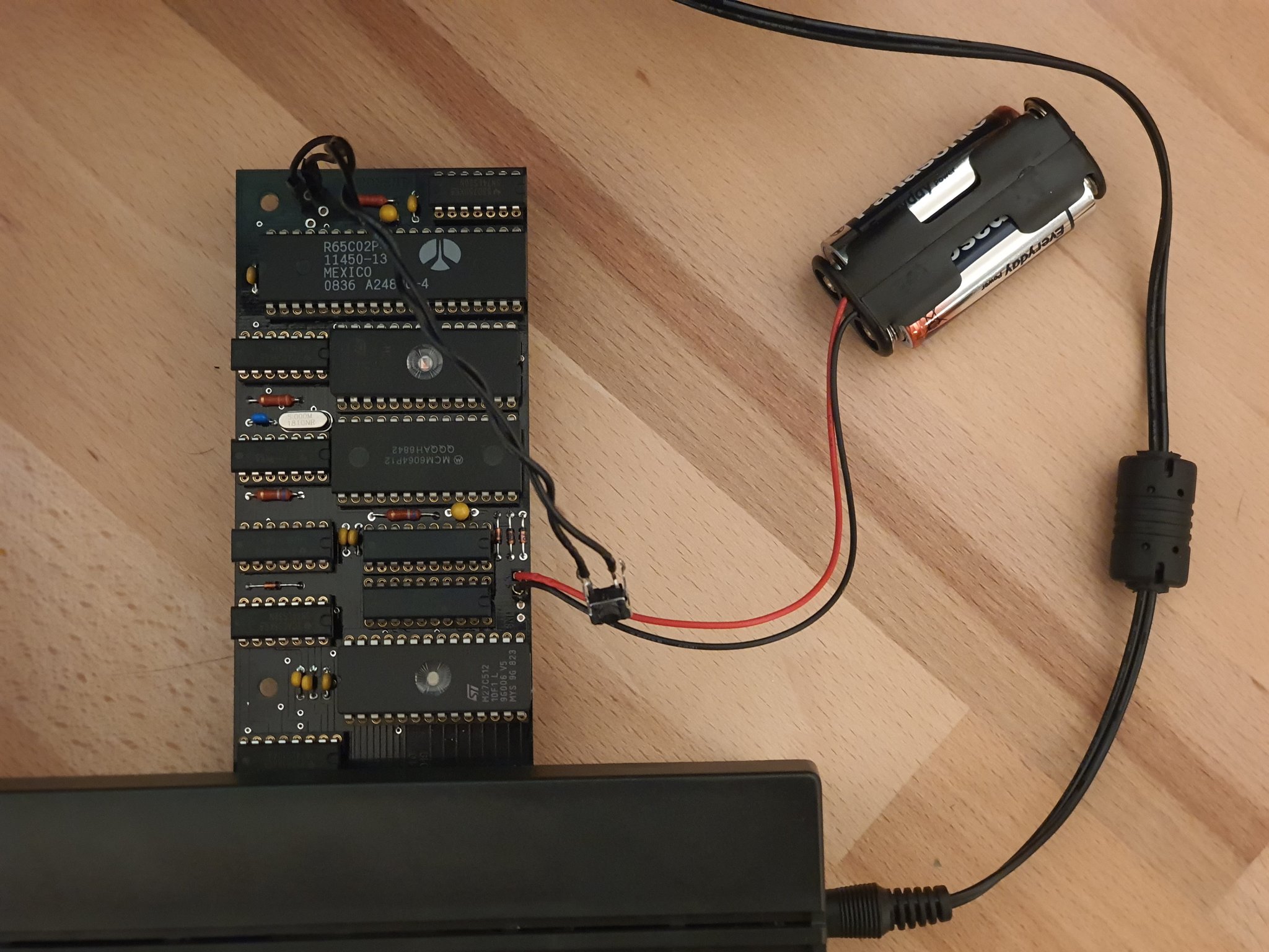
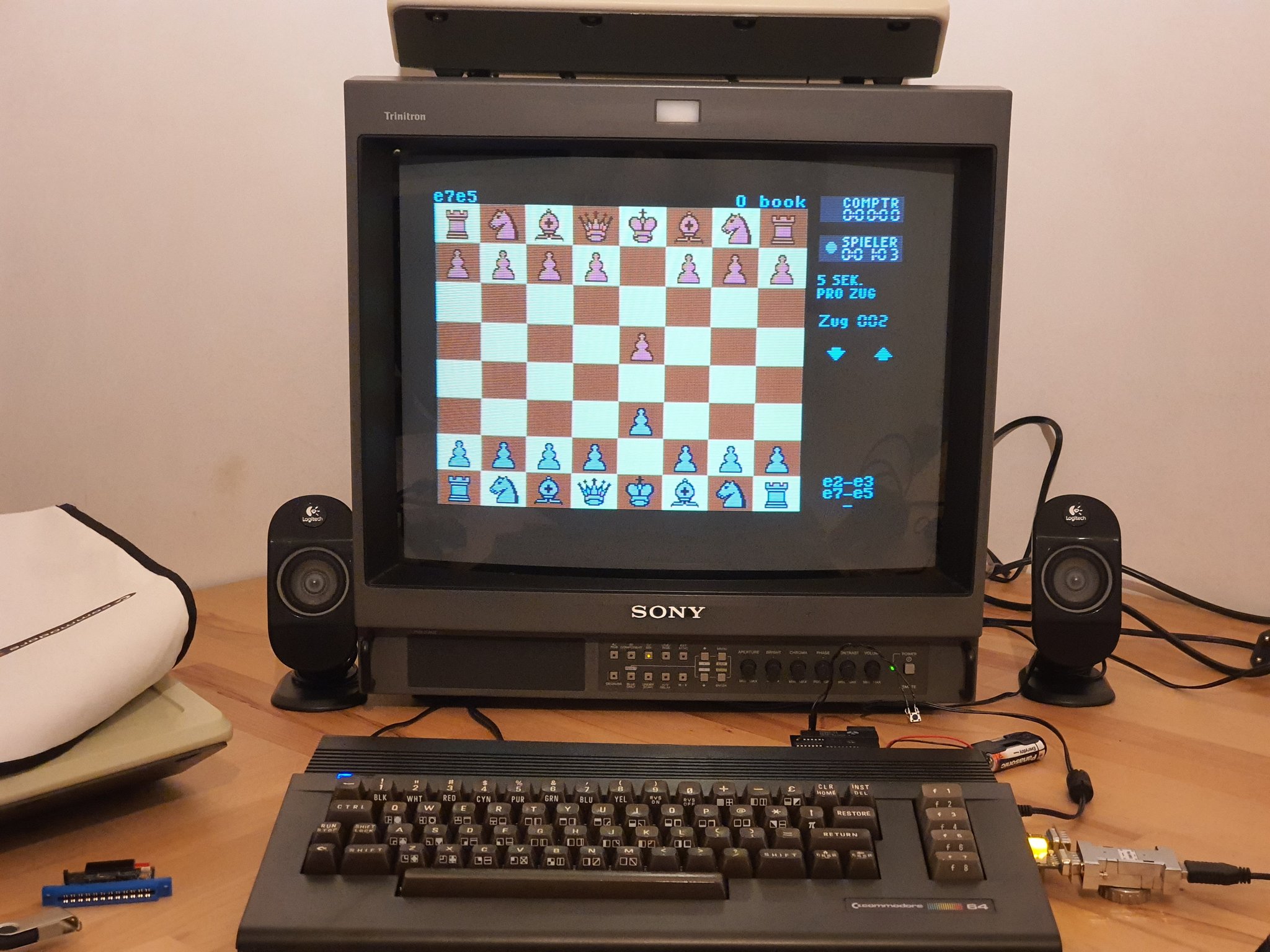
The PCB Rev 1.0 has been prototyped by Amon_RA on twitter. Thank you so much! Here are two images from his setup:
| Image 1 | Image 2 |
|---|---|
 |  |
The Rev 1.0 had a grounded READ pin near the top edge. To find it look at the 74LS32 closest to the CPU, pin 8. If you have Rev 1.0, cut this trace betwen pin8 and GND at top edge. This is fixed in Rev 1.1
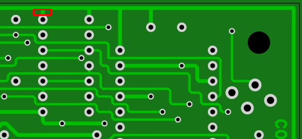
I would also like to thank the work by lvr for the schematics draft he posted in a forum64.de thread. With this schematic I was able to match my gerbers against a netlist generated from his schematics, and in this way the error in Rev 1.0 was easy to spot. The draft was very close to the layout. Thanks also to @thilographie_de for hunting the error with me.
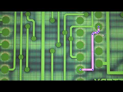
After doing the C64 KU-motherboard and the videoseries, I still hadn't shown my viewers how I went from images to gerber files. This is where I got the motivation for doing this TFCC replica. I made two videos. The first video got linked on Jani's website and also ended up in an article about it on hackaday called Reverse Engineer PCBs With SprintLayout. :-)
The replica above I'd like to be .. a replica. Some changes are desired. In this KiCad version we have moved two ICs back onto the grid. They were just too close for IC sockets. A zener diode was also too close to the same ICs. The crystal touched some metal. The power rails were thin. I have solved the changes in this version. The schematics were drafted by lvr as mentioned above regarding the PCB Rev 1.0.
Gerbers are available. Look under the KiCad folder.
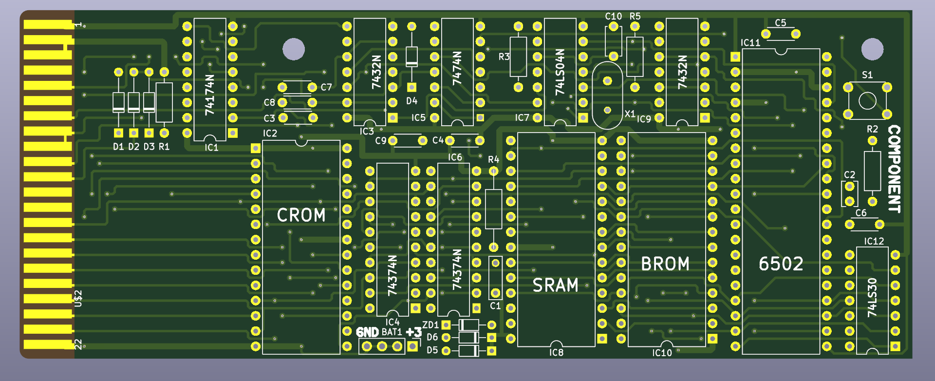
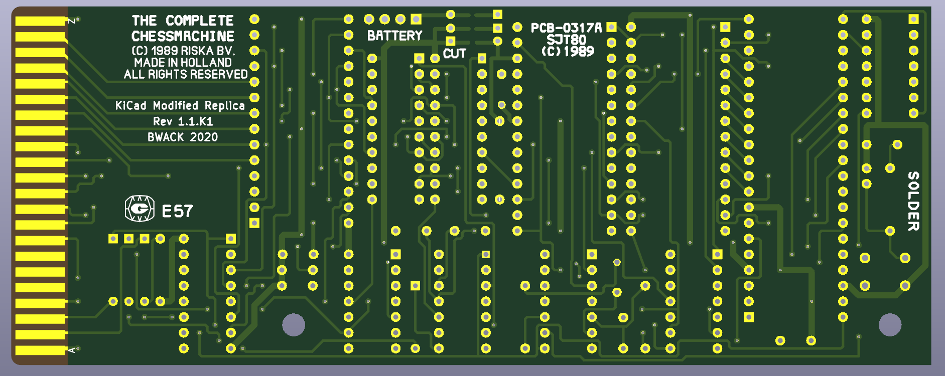
The KiCad version branches off from the replica 1.1 board, hence why it is called 1.1.K1 where K is KiCad :)
Note that this version has never been prototype. Use at own risk if you decide to do so!
| Qty | Value | Footprint | References |
|---|---|---|---|
| 4 | 100n | Capacitor_THT:C_Disc_D4.3mm_W1.9mm_P5.00mm | C3, C4, C5, C6 |
| 4 | 1N4148 | Diode_THT:D_DO-34_SOD68_P10.16mm_Horizontal | D1, D2, D3, D4 |
| 3 | 1n | Capacitor_THT:C_Disc_D4.3mm_W1.9mm_P5.00mm | C7, C8, C9 |
| 2 | 1N4148 | Diode_THT:D_DO-34_SOD68_P7.62mm_Horizontal | D5, D6 |
| 2 | 2k2 | Resistor_THT:R_Axial_DIN0207_L6.3mm_D2.5mm_P10.16mm_Horizontal | R1, R2 |
| 2 | 3.7mm | MountingHole:MountingHole_3.7mm | H1, H2 |
| 2 | 7432N | Package_DIP:DIP-14_W7.62mm | IC3, IC9 |
| 2 | 74374N | Package_DIP:DIP-20_W7.62mm | IC4, IC6 |
| 1 | 1u | Capacitor_THT:C_Rect_L7.0mm_W2.0mm_P5.00mm | C1 |
| 1 | 1u | Capacitor_THT:C_Rect_L4.0mm_W2.5mm_P2.50mm | C2 |
| 1 | 2V7 | Diode_THT:D_DO-34_SOD68_P7.62mm_Horizontal | ZD1 |
| 1 | 330 | Resistor_THT:R_Axial_DIN0207_L6.3mm_D2.5mm_P10.16mm_Horizontal | R5 |
| 1 | 560p | Capacitor_THT:C_Disc_D4.7mm_W2.5mm_P5.00mm | C10 |
| 1 | 5MHz | Crystal:Crystal_HC49-U_Vertical | X1 |
| 1 | 6502 | Package_DIP:DIP-40_W15.24mm | IC11 |
| 1 | 680 | Resistor_THT:R_Axial_DIN0207_L6.3mm_D2.5mm_P15.24mm_Horizontal | R4 |
| 1 | 680 | Resistor_THT:R_Axial_DIN0207_L6.3mm_D2.5mm_P10.16mm_Horizontal | R3 |
| 1 | 74174N | Package_DIP:DIP-16_W7.62mm | IC1 |
| 1 | 7474N | Package_DIP:DIP-14_W7.62mm | IC5 |
| 1 | 74LS04N | Package_DIP:DIP-14_W7.62mm | IC7 |
| 1 | 74LS30 | Package_DIP:DIP-14_W7.62mm | IC12 |
| 1 | CARTRIDGE | library:C64_EXPANSION_PORT | U$2 |
| 1 | MA04-1 | Connector_PinHeader_2.54mm:PinHeader_1x04_P2.54mm_Vertical | BAT1 |
| 1 | RESET | Button_Switch_THT:SW_TH_Tactile_Omron_B3F-10xx | S1 |
| 1 | ROM1 | Package_DIP:DIP-28_W15.24mm | IC2 |
| 1 | ROM2 | Package_DIP:DIP-28_W15.24mm | IC10 |
| 1 | SRAM | Package_DIP:DIP-28_W15.24mm | IC8 |
It measures 148.9 × 58.1 mm and has 2 copper layers, 1.6 mm thick.
40 parts, built around the 74LS30PC. The full list of its parts is on this page, with links to each part's symbol and footprint where PCBKit's library has them.
From the bwack/TheFinalChessCard repository on GitHub, at the commit this page was made from: the board is KiCad/finalchesscard_lvr_draft1/finalchesscard_lvr_draft1.kicad_pcb. PCBKit opens the board in the browser, with nothing to install.
Its repository states no licence, so its author keeps all rights: ask bwack before reusing the design.
jotego/jtcores
FPGA cores compatible with multiple arcade game machines and KiCAD schematics of arcade games. Working on MiSTer FPGA/Analogue Pocket


SukkoPera/OpenC64KernalCart
Open Hardware Multi-KERNAL Cartridge for the Commodore 64


yanataka60/MZ80K_SD
MZ-80KシリーズでSD-CARDからのアプリケーション起動、BASICなどのアプリケーションからSD-CARDへのロード、セーブを実現するものです

