
2 layers22.2 × 46.4 mm
C64-Switchless Quad Kernal Switcher
bwack/C64-Switchless-Multi-Kernal-27C256-adapter
Kernal switcher for the C64/C64C/C128
14 parts112
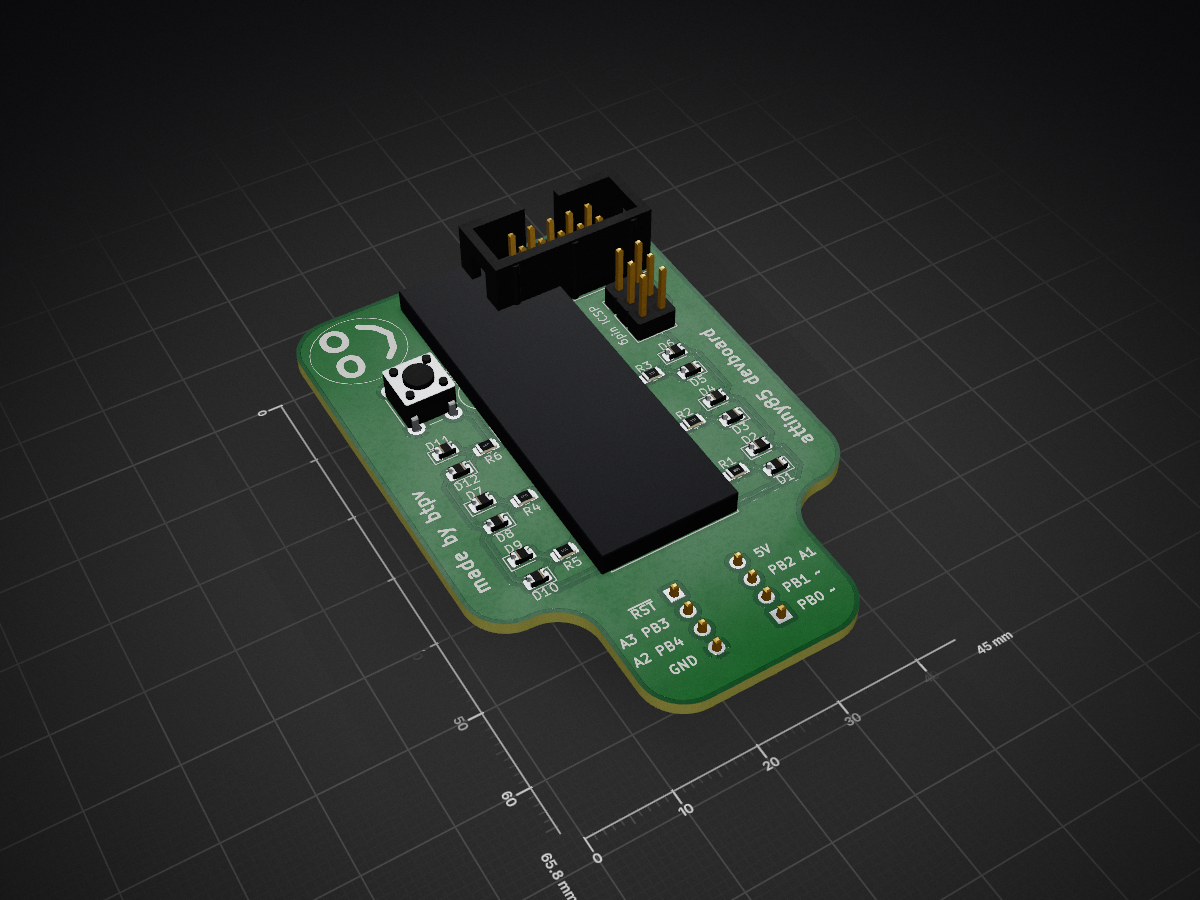
 btpv/attiny85dev
Attiny85dev is an open-source printed circuit board by btpv, from the btpv/attiny85dev repository on GitHub. It is a 2-layer board of 45 × 65.8 mm with 24 parts on 16 nets, routed with 193 tracks and 0 vias.
It is built around the ATTINY85-20PU. Its parts include 12 diodes, 6 resistors, 4 connectors, 1 IC and 1 switch. It belongs with the AVR (ATmega, ATtiny) boards of this library.
| Qty | Value | Footprint | References |
|---|---|---|---|
| 12 | LED | Diode_SMD:D_0805_2012Metric | D1, D2, D3, D4, D5, D6, D7, D8, D9, D10, D11, D12 |
| 6 | 330 | Resistor_SMD:R_0805_2012Metric | R1, R2, R3, R4, R5, R6 |
| 1 | 10pin ICSP | Connector_IDC:IDC-Header_2x05_P2.54mm_Vertical | J4 |
| 1 | 6pin ICSP | Connector_PinHeader_2.54mm:PinHeader_2x03_P2.54mm_Vertical | J3 |
| 1 | ATtiny85-20P | Socket:DIP_Socket-14_W4.3mm_W5.08mm_W7.62mm_W10.16mm_W10.9mm_3M_214-3339-00-0602J | U1 |
| 1 | Conn_01x04_Pin | Connector_PinHeader_2.54mm:PinHeader_1x04_P2.54mm_Vertical | J2 |
| 1 | breadboard | Connector_PinHeader_2.54mm:PinHeader_1x04_P2.54mm_Vertical | J1 |
| 1 | reset | Button_Switch_THT:SW_PUSH_6mm | SW1 |
It measures 45 × 65.8 mm and has 2 copper layers, 1.6 mm thick.
24 parts, built around the ATTINY85-20PU. The full list of its parts is on this page, with links to each part's symbol and footprint where PCBKit's library has them.
From the btpv/attiny85dev repository on GitHub, at the commit this page was made from: the board is attiny85dev.kicad_pcb and its schematic attiny85dev.kicad_sch. PCBKit opens the board in the browser, with nothing to install.
Its repository states no licence, so its author keeps all rights: ask btpv before reusing the design.
bwack/C64-Switchless-Multi-Kernal-27C256-adapter
Kernal switcher for the C64/C64C/C128

plusvic/simplebus2-intercom
General description of the Simplebus2 protocol used by some Comelit's intercoms. Hardware for retransmitting Simplebus2 messages over UART.

osmocom/osmocom-analog
Software Implementation of analog cellular telephony systems like NMT, TACS, IMTS, A/B/C-Netz; mirror of https://gitea.osmocom.org/cellular-infrastructure/osmocom-analog

strickyak/jerboa-attiny85-mod-synth
Modular Synthesizer using an ATtiny85 chip for each module.


Hack-a-Day/Remoticon_KiCad_Blender
support files for the 2020 Remoticon KiCad to Blender > PCB renders workshop
