


4 layers80 × 73.8 mm
ESP32-Bit Pirate Dock
AndreiVladescu/ESP32-Bit-Pirate-Hardware
Carrier breaker-board for the ESP32-S3 Devkit. Works great with the ESP32-Bit-Pirate firmware.
49 parts85CERN-OHL-W-2.0

 brainstorm/FlashCAT-P30-Header
FlashCAT header that should accept StrataFlash PC28F256P30T85A
Flashcat p30 is an open-source printed circuit board by brainstorm, from the brainstorm/FlashCAT-P30-Header repository on GitHub. It is a 4-layer board of 51 × 33 mm with 15 parts on 62 nets, routed with 416 tracks and 72 vias.
It is built around the PC28F256P30T85A, TLV75518PDBV and RC0603FR-0710KL. Its parts include 9 capacitors, 2 resistors, 2 ICs and 2 connectors.


KiCad 10 project for a FlashcatUSB (Mach1 / XPORT) parallel adapter that reads
and writes Intel / Micron StrataFlash P30 parallel NOR in the 64-ball
Easy BGA package (e.g. PC28F256P30T85, RC28F256P30T85; the JS28F…
parts are TSOP-56 and need the TSOP adapter instead), using an HMILU
BGA64-1.0-TP21NS open-top socket made for 10 × 13 mm BGA-64 parts, as
discussed with Embedded Computers (thread "256P30T", Oct 2020 – Feb 2021).
Rev C; rev B used a Sensata CBG064-087G, whose nest is for 11 × 13 mm parts.
| Top (socket) | Bottom (all SMD parts) |
|---|---|
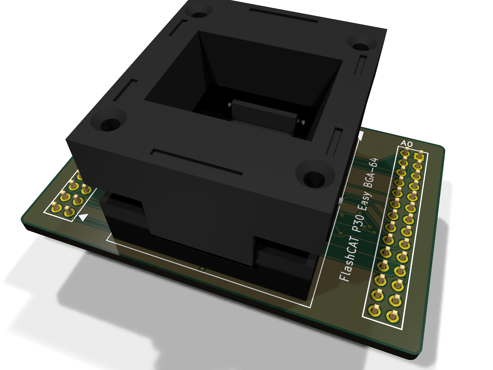 | 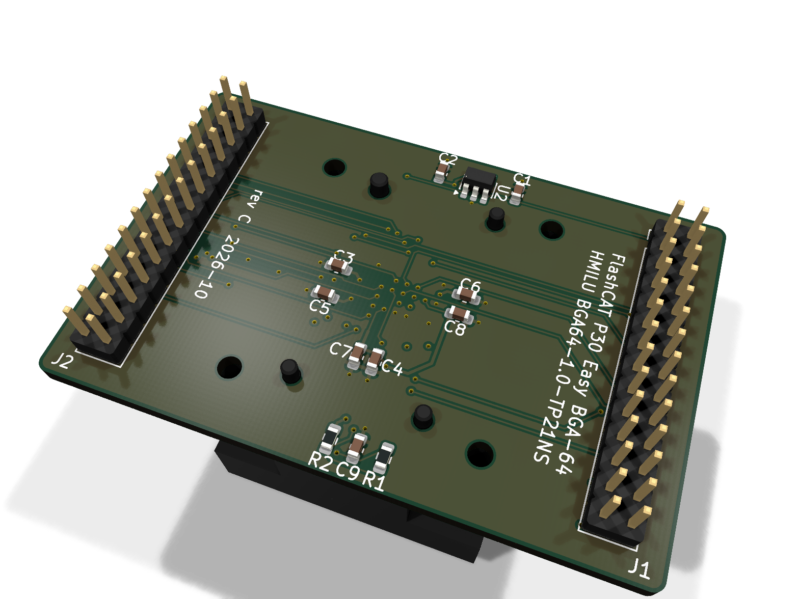 |
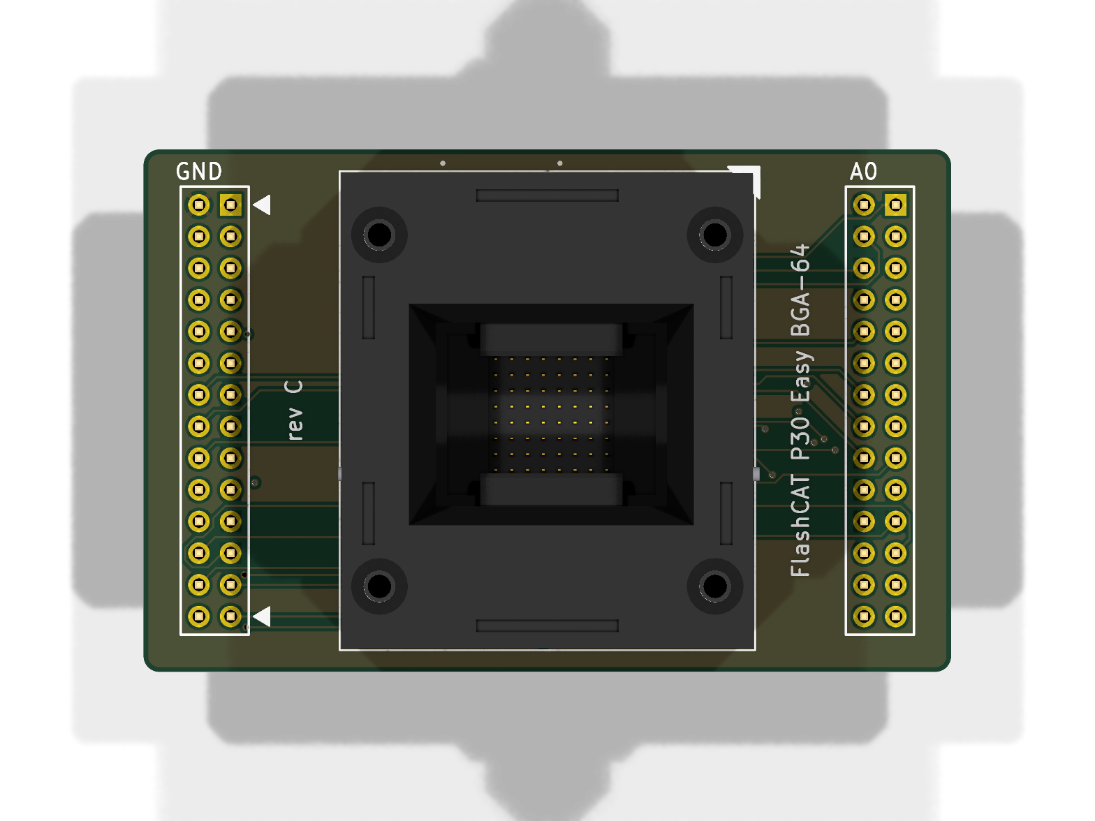 | 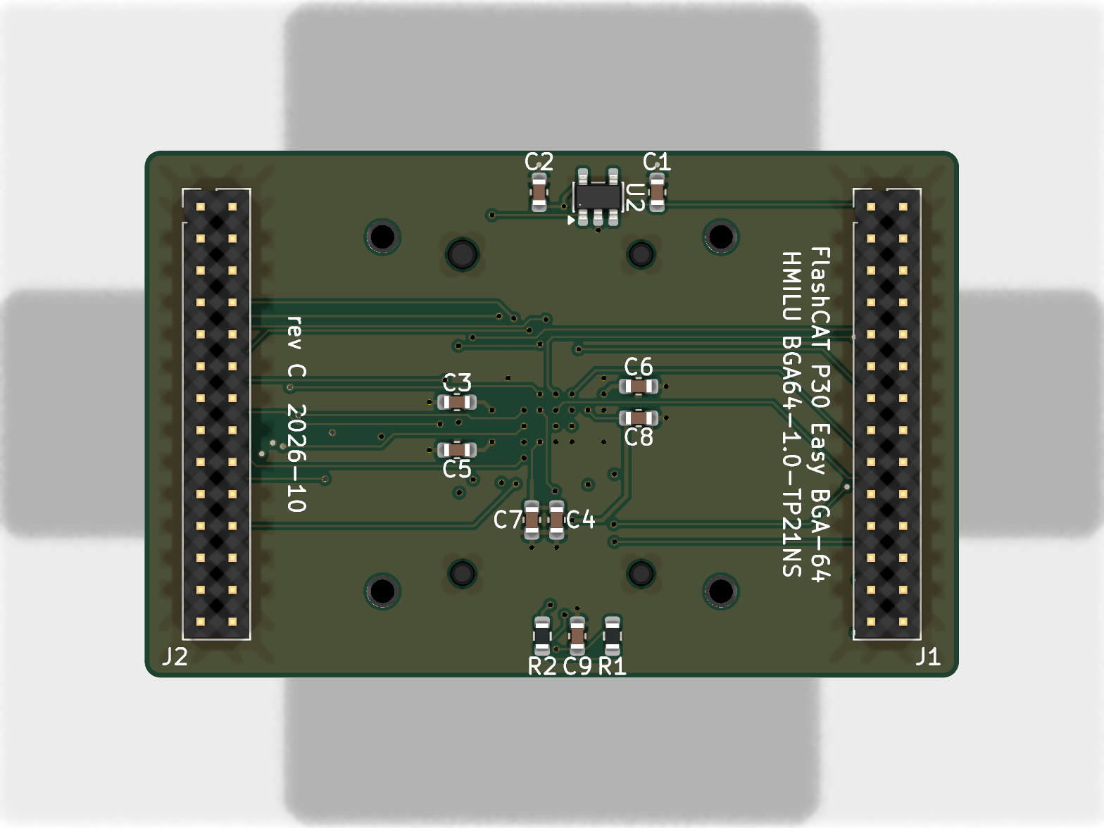 |
| Side | Decoupling at the socket balls (bottom) |
|---|---|
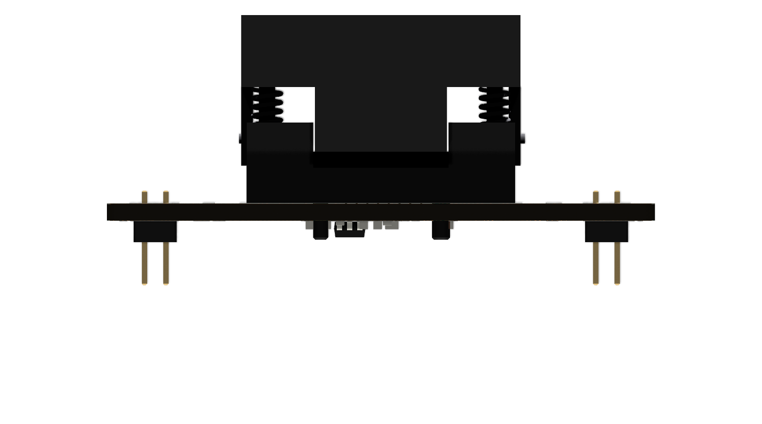 | 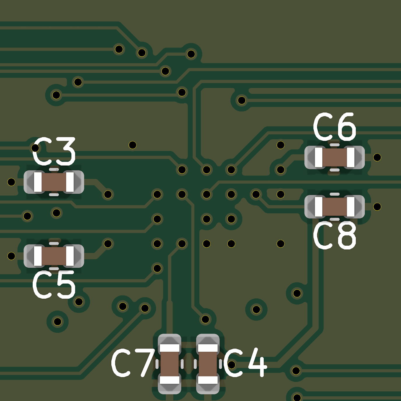 |
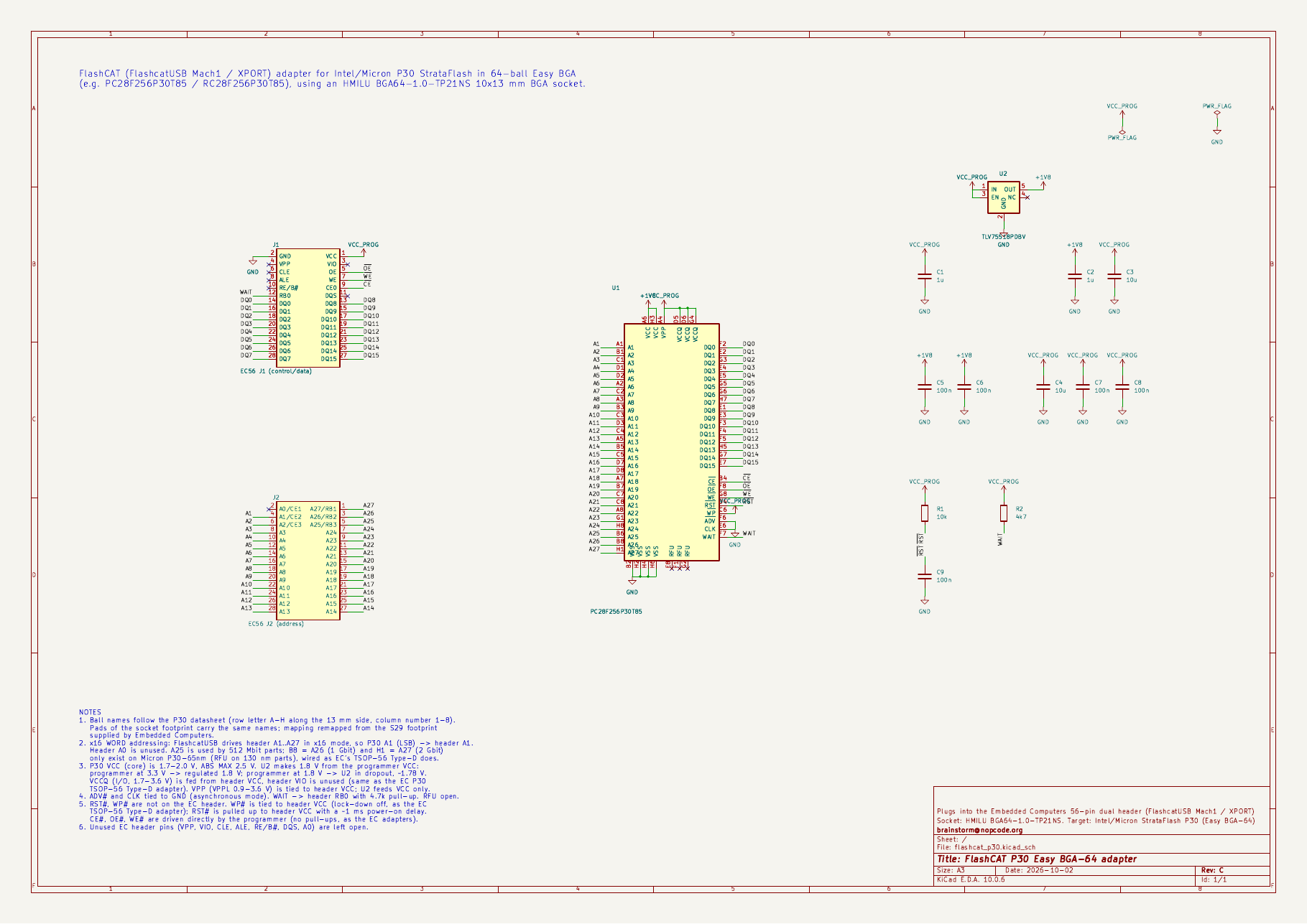
Schematic as PDF: fab/docs/schematic.pdf ·
Gerbers: fab/flashcat_p30-gerbers.zip
hardware/
  flashcat_p30.kicad_pro / .kicad_sch / .kicad_pcb   the project
  lib/flashcat_p30.kicad_sym                         P30 socket, EC header, LDO, R, C, power symbols
  lib/flashcat_p30.pretty/HMILU_BGA64-1.0-TP21NS     socket footprint, pads named with P30 ball names
  lib/flashcat_p30.3dshapes/HMILU_BGA64-1.0-TP21NS.step  socket 3D model (built from the HMILU drawing)
  fab/                                               gerbers (+zip), drill, BOM, CPL, PDFs
  renders/                                           3D renders, schematic preview, sheet view
tools/ generators + checks (source of truth: design.py)| P30 ball(s) | Signal | Connected to |
|---|---|---|
| A1…A25 | address (A1 = LSB, word address) | EC header A1…A25 (header A0 unused) |
| B8 / H1 | RFU on 130 nm parts; A26 / A27 on Micron P30-65nm 1 / 2 Gbit | EC header A26/RB2 / A27/RB1 |
| DQ0…DQ15 | data | EC header DQ0…DQ15 |
| CE#, OE#, WE# | control | EC header CE0, OE, WE (driven directly, no pull-ups) |
| RST# | reset | 10k to VCC + 100 nF to GND (~1 ms power-on reset) |
| WP# | write protect | tied to header VCC (lock-down disabled) |
| ADV#, CLK | sync-burst inputs | GND (asynchronous mode, per datasheet) |
| WAIT | wait/ready | EC header RB0, 4.7k pull-up to VCC |
| RFU (E8, F1, G2) | – | open |
| VCC ×2 | core 1.7–2.0 V | +1V8 from U2 (TLV75518) – the LDO feeds only these |
| VPP | program/erase supply | header VCC (3.3 V) |
| VCCQ ×3 | I/O 1.7–3.6 V | header VCC (header VIO unused) |
| VSS ×4 | ground | GND |
Why these choices — cross-checked against the author's own TSOP-56 Type-D
adapter ("Supports P30 and P33 Strataflash devices such as 28F256P30",
schematic SCM_TSOP56_D.png on the EC parallel adapters page):
| EC TSOP-56 Type-D (P30) | this board | |
|---|---|---|
| Core VCC | MIC5504 1.8 V LDO from header VCC, 3 × 1 µF | TLV75518 1.8 V LDO (same SOT-23-5 pinout; MIC5504-1.8YM5 is a drop-in) |
| VCCQ | header VCC | header VCC |
| Header VIO | unused | unused |
| WAIT | → RB0, 4.7k pull-up to VCC | same |
| CLK, ADV# | GND | GND |
| WP# | tied to VCC | tied to VCC |
| RST# | tied to VCC | 10k pull-up to VCC + 100 nF (~1 ms power-on reset) |
| TSOP pin 13 / pin 28 | wired to header A27/RB1 and A26/RB2 (see note) | Easy BGA B8 → A26/RB2, H1 → A27/RB1 (same idea) |
| VPP | VCC rail | header VCC |
| CE#, WE# pull-ups | none | none |
| Address | P30 A1 → header A1/CE2 … A25 → A25/RB3 | same, plus A26/A27 |
Verified in the Type-D schematic: header VCC (pin 28) → MIC5504 VIN and
EN, VOUT (P$5) → C3 1 µF → TSOP pin 33 VCC, part marked "1.8V LDO".
Note: on that drawing TSOP pin 13 is labelled VCC_A27 and routed to
header A27/RB1, and pin 28 to header A26/RB2. That matches Micron's
P30-65nm TSOP pinout (512 Mbit–1 Gbit): pin 28 is A26 there (VSS on
the 130 nm parts) and pin 13 became RFU (VCC on 130 nm). The Easy BGA
equivalent is below.
Is the LDO needed? Yes. None of the other EC adapters carry a regulator because they are all for 3 V (or 5 V) core parts; the only adapter on the page with an LDO is the P30 one, for exactly the reason below. (The other small ICs on those schematics are a VPP load switch on DIP-40 and push-pull/open-drain MOSFETs on BGA-153, not regulators.)
Addressing: the FlashcatUSB firmware/software drives the header in x16 NOR
mode as "Addressing is done A1-A27 (WORD ADDR)" (Parallel_NOR_NAND.vb,
E_EXPIO_WRADDR.Parallel_X16). P30 names its LSB A1, so An → header
An — the "same pin connection as the TSOP56" the author mentioned.
A25 is wired so 512 Mbit dual-die P30 parts work too.
Micron P30-65nm (1 Gbit / 2 Gbit) uses the same Easy BGA ballout but
puts A26 on ball B8 and A27 on ball H1 (die select on the 2 Gbit
dual-die part), balls that are RFU on the 130 nm Intel/Numonyx datasheet.
Both are wired straight to header A26/RB2 and A27/RB1 so PC28F00AP30…
and PC28F00BP30… parts work. On 130 nm parts those balls are unused
inside the package, so the programmer driving them is expected to be
harmless (the datasheet asks to treat RFU as do-not-connect, and EC's TSOP
Type-D adapter makes the same trade-off). Needs FlashcatUSB to know the
part; 65 nm parts also need ≥ 300 µs from VCC valid to RST# high, which
the ~1 ms RC covers.
Core voltage: P30 VCC is 1.7–2.0 V with an absolute maximum of 2.5 V,
while the header VCC runs at 3.3 V for these adapters (the author's MIC5504
needs ≥ 2.5 V in, so their design assumes 3.3 V too). Wiring VCC straight
to the header would destroy the chip. U2 (TLV755P, 1.45–5.5 V input) was
kept over the MIC5504 because it also survives a 1.8 V programmer setting:
it just drops out and passes ~1.78 V through.
VPP goes to header VCC (3.3 V), like the author's adapter. VPPL is 0.9–3.6 V, but program/erase timings are specified at the higher end, and this keeps the LDO dedicated to the core VCC balls. The header's VPP pin (which can carry 12 V for old EPROMs) is deliberately left unconnected.
tools/fanout.py): rings 1+2 on
F.Cu, ring 3 on B.Cu, the centre balls on In2 (VCCQ D5 is linked to its
VCCQ neighbour D6 instead of escaping), one 0.127 mm track per channel;
each escape exits on the side facing its header (data → J1, address → J2);
B.Cu channels next to A4/A6/H3/G4 are kept free for the bottom decap traces,
and a locked B.Cu link joins the two VCCQ cap groups onto one VCC via. Balls
that leave the top layer (inner escapes, GND balls, decap balls) do so
through a 0.3/0.5 mm via in the centre of their pad (23 pads), which
has to be resin filled and copper capped (see fabrication spec); GND
balls drop straight into the In1 plane that way. D3 (A11) and F4 (DQ11)
escape sideways towards their header pins, and A2, DQ11, DQ12 and WAIT are
pre-routed by hand (design.PREROUTES): Freerouting otherwise walled
their header pins in. The rest was autorouted with Freerouting and
cleaned up (dangling stubs and pad vias it made redundant removed).EC_56P_HEADER.png. Top-silk "GND" and "A0" mark the
first pins; all silkscreen reads the same way as the programmer's. As on
EC's own adapters (TSOP-56 Type-D, BGA-64 photos on their
parallel adapters page),
each header has a top-silk outline box and two solid "◄" triangles sit on
the inner side of the data header (J1) at its first and last row, to line
the adapter up with the matching mark on the FlashcatUSB.BGA64_EasyBGA_Pinout.png) is the J3-style ballout
(VPEN, STS, BYTE#, CE0–CE2, RP#): it powers the core from 3 V, leaves
P30's ADV#/CLK/VCCQ(D5, D6) balls on RFU pins, and would over-voltage a P30
core. That is why this custom board is needed.| Ref | Qty | Part | Notes |
|---|---|---|---|
| U1 | 1 | HMILU BGA64-1.0-TP21NS BGA-64 1.0 mm socket, 10 × 13 mm | solderless: screwed onto the board after assembly; not in the CPL. 3D model in lib/flashcat_p30.3dshapes/ |
| J1, J2 | 2 | 2×14 male header, 2.00 mm pitch (e.g. Samtec TMM-114-01-G-D) | mount on bottom |
| U2 | 1 | TI TLV75518PDBVR (SOT-23-5) | 1.8 V LDO, 1.45 V min input; alt. Microchip MIC5504-1.8YM5 (same pinout, needs ≥ 2.5 V in) |
| C1, C2 | 2 | 1 µF 25 V X5R 0603 (GRM188R61E105KA12D) | LDO in / out, either side of U2 |
| C3 | 1 | 10 µF 10 V X5R 0603 (GRM188R61A106KE69D) | bottom, at ball A4 (VPP, header VCC) |
| C5, C6 | 2 | 100 nF 16 V X7R 0603 (GRM188R71C104KA01D) | bottom, at balls A6 / H3 (VCC, +1V8) |
| C4, C7 | 2 | 10 µF + 100 nF 0603 | bottom, at balls D5/D6 (VCCQ) |
| C8 | 1 | 100 nF 0603 | bottom, at ball G4 (VCCQ) |
| C9 | 1 | 100 nF 0603 | RST# power-on RC |
| R1 | 1 | 10 kΩ 1 % 0603 (RC0603FR-0710KL) | RST# pull-up (with C9: power-on reset) |
| R2 | 1 | 4.7 kΩ 1 % 0603 (RC0603FR-074K7L) | WAIT → RB0 pull-up |
All SMD parts are on the bottom side (single-sided SMD assembly; the top
carries only the socket). The socket decoupling caps (C3–C8) sit 1–2 mm
from their VCC/VCCQ/VPP balls, each with its own short trace from the ball
and its own GND via into the In1 plane; the LDO (U2) with C1/C2, the
WAIT pull-up and the RST# RC sit in the strips above/below the socket. Reflow
the bottom, hand-solder the headers, then screw the socket on (no solder on
its pads). fab/assembly/
has a generic BOM plus JLCPCB-style bom_jlc.csv / cpl_jlc.csv; placement
coordinates are relative to the socket centre (board aux origin). Add LCSC
part numbers for your assembler before ordering. Check CPL rotations in the
assembler's preview.
| Item | Value | Source |
|---|---|---|
| Layers / material | 4 layers, FR-4, 1.6 mm, 1 oz outer copper | design choice |
| Track / space | min 0.127 / 0.127 mm (power 0.2–0.3 mm) | design choice; JLCPCB multilayer minimum is 0.09 / 0.09 mm [1] |
| Vias | 0.3 mm drill / 0.5 mm pad, min via-to-via hole gap on the board 0.37 mm | JLCPCB: via ≥ 0.15/0.25 mm, via hole-to-hole ≥ 0.2 mm [1] |
| Socket pads | 64 × Ø0.55 mm solid SMD pads, mask open, no paste | HMILU drawing ("64-Ø0.55 实心焊盘", contact tip detail) |
| Via-in-pad | 23 socket pads have a 0.3/0.5 mm via in their centre: these must be epoxy filled and copper capped | design choice (see below); JLCPCB: "Vias can be placed within BGA pads using filled and plated-over vias" [1] |
| Surface finish | ENIG | design choice: flat pads for the spring contacts (HASL leaves domed pads) |
| Locator holes | NPTH 3 × Ø1.53, 1 × Ø1.83 mm | HMILU drawing (Ø1.45 / Ø1.75 +0.05/−0) + JLCPCB hole tolerance +0.13/−0.08 mm [1] |
| Fixing holes | NPTH 4 × Ø2.00 mm | HMILU drawing |
| Silkscreen | text ≥ 1.0 mm high, ≥ 0.15 mm stroke | JLCPCB legend minimum [1] |
[1] JLCPCB PCB capabilities, https://jlcpcb.com/capabilities/pcb-capabilities (checked 2026-10-03).
Why via-in-pad (design choice, not from the HMILU drawing). The drawing only defines the pad pattern. The pads are SMD, so balls that cannot escape on the top layer (inner balls, GND, decoupled power balls) need a via; it was put in the pad centre because the 1.0 mm grid has no room for dog-bone vias next to every inner pad. A filled and capped via leaves a flat pad; an open or merely tented via would leave a hole or dimple under the spring contact. Confirm with HMILU / your reseller that filled vias under the contacts are fine if in doubt.
fab/flashcat_p30-gerbers.zip (Gerbers + PTH/NPTH Excellon).fab/assembly/bom_jlc.csv +
cpl_jlc.csv; the socket (U1) is not assembled, the headers are
hand-soldered. Check part rotations in the assembler's preview.tools/verify.py: ball/header mapping 0 errors · ERC 0 · DRC 0 violations,
0 unconnected (all severities) · schematic ↔ PCB parity 0.
cd hardware/tools
python3 gen_libs.py     # symbols + socket footprint (references the 3D model)
../build/cqenv/bin/python make_socket_3d.py   # socket STEP model (CadQuery, Python 3.12 venv)
python3 gen_pro.py      # project, rules, net classes
python3 gen_sch.py      # schematic
python3 gen_pcb.py      # placement, nets, planes, silk (from schematic netlist)
python3 route.py        # fanout + Freerouting 2.4.1 (Java 25; FR_VERSION=2.1.0 for Java 21)
                        #   + stub trim + pours + fill, retries until 0 unconnected
python3 center.py       # move board to the middle of the A4 sheet, aux/grid origin = socket centre
python3 verify.py       # mapping + ERC + DRC with schematic parity
python3 make_fab.py     # gerbers, drill, BOM, CPL, PDFs
design.py is the single source of truth for the ballout, header pinout,
socket geometry and nets. Once hand-edited in KiCad, the .kicad_* files
become the master copy and the generators should not be re-run.
No vendor model is published for the BGA64-1.0-TP21NS, so
tools/make_socket_3d.py builds a simplified STEP from the HMILU drawing's
top, front-section and isometric views: a base with four corner towers
(3.3 mm slab, towers to 7.5 mm) and the 10 × 13 mm IC holder between them; a
26 × 30 mm cover (10.8–17.5 mm, cover up) with an 18 × 14 mm funnel window,
countersunk corner holes and a skirt in the middle of each side that drops
between the towers (with the guide slot and pin on the 30 mm faces); coil
springs on the towers around the corner screw posts; the two clamp arms
(levers on pins beside the IC holder, hook tips resting on the chip's 13 mm
edges, as in the drawing's top and side views); 64 contact blades down
to the pads and the four locator pins (3.4 mm). Hole, pin and contact
positions come from design.py, so they match the footprint exactly;
proportions the drawing does not dimension were measured from it. It is for
fit/clearance checks and renders, not a manufacturer-accurate model.
| Qty | Value | Footprint | References |
|---|---|---|---|
| 5 | 100n | Capacitor_SMD:C_0603_1608Metric | C5, C6, C7, C8, C9 |
| 2 | 10u | Capacitor_SMD:C_0603_1608Metric | C3, C4 |
| 2 | 1u | Capacitor_SMD:C_0603_1608Metric | C1, C2 |
| 1 | 10k | Resistor_SMD:R_0603_1608Metric | R1 |
| 1 | 4k7 | Resistor_SMD:R_0603_1608Metric | R2 |
| 1 | EC56 J1 (control/data) | Connector_PinHeader_2.00mm:PinHeader_2x14_P2.00mm_Vertical | J1 |
| 1 | EC56 J2 (address) | Connector_PinHeader_2.00mm:PinHeader_2x14_P2.00mm_Vertical | J2 |
| 1 | PC28F256P30T85 | flashcat_p30:HMILU_BGA64-1.0-TP21NS | U1 |
| 1 | TLV75518PDBV | Package_TO_SOT_SMD:SOT-23-5 | U2 |
It measures 51 × 33 mm and has 4 copper layers, 1.6 mm thick.
15 parts, built around the PC28F256P30T85A, TLV75518PDBV and RC0603FR-0710KL. The full list of its parts is on this page, with links to each part's symbol and footprint where PCBKit's library has them.
From the brainstorm/FlashCAT-P30-Header repository on GitHub, at the commit this page was made from: the board is hardware/flashcat_p30.kicad_pcb and its schematic hardware/flashcat_p30.kicad_sch. PCBKit opens the board in the browser, with nothing to install.
Its repository states no licence, so its author keeps all rights: ask brainstorm before reusing the design.
AndreiVladescu/ESP32-Bit-Pirate-Hardware
Carrier breaker-board for the ESP32-S3 Devkit. Works great with the ESP32-Bit-Pirate firmware.

marqs85/DExx-vd_isl
Advanced video digitizer add-on module for Terasic DE series FPGA development boards.


Envious-Data/EnvOpenAudio
An open source headphone/PC speaker project utilizing the RP2040, UDA1334A and TPA2016


Orlandogani/pers-esp32-headset
This project was made by kicad 10.0. My first personal headset to support my several research in audio or embedded fields

pustowhite/rp2040-logic-analyzer
An 8-channel RP2040 logic analyzer PCB designed in KiCad, with USB-C and selectable 1.8 V / 3.3 V input logic modes.