2 layers130.3 × 85.3 mm
Lapka ChocV1V2 Solder
braindefender/lapka
Wireless ergonomic split keyboard for those who have paws (:
21 parts131CC-BY-SA-4.0

 braindefender/lapka131
Wireless ergonomic split keyboard for those who have paws (:
Lapka ChocV2 Solder is an open-source printed circuit board by braindefender, from the braindefender/lapka repository on GitHub, published under the CC-BY-SA-4.0 licence. It is a 2-layer board of 130.3 × 85.3 mm with 21 parts on 25 nets, routed with 188 tracks and 47 vias.
Its parts include 18 switches and 1 IC. It belongs with the keyboards and input boards of this library.
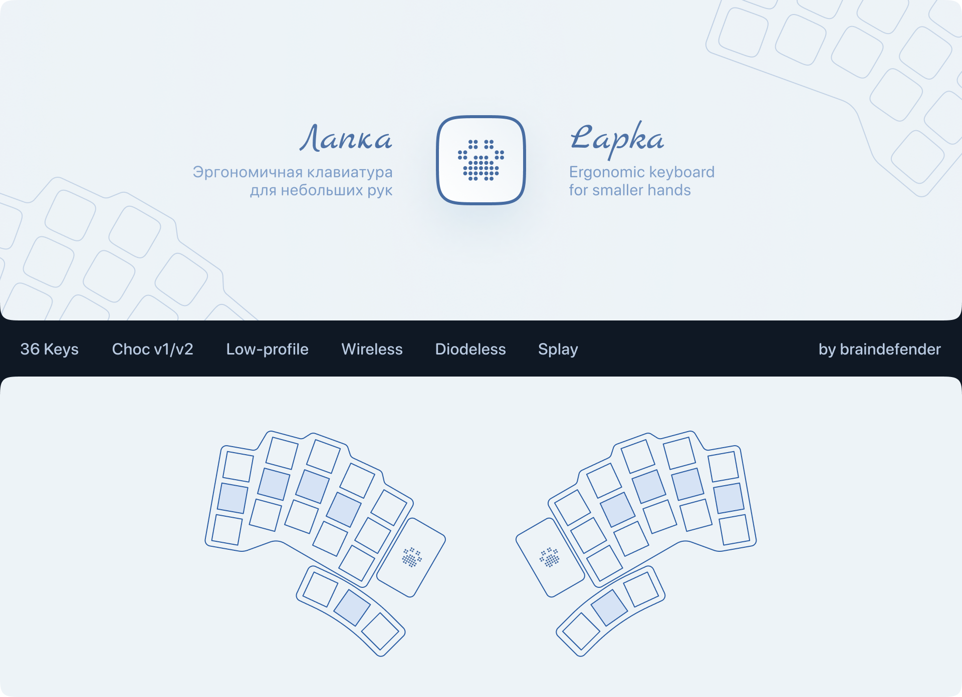
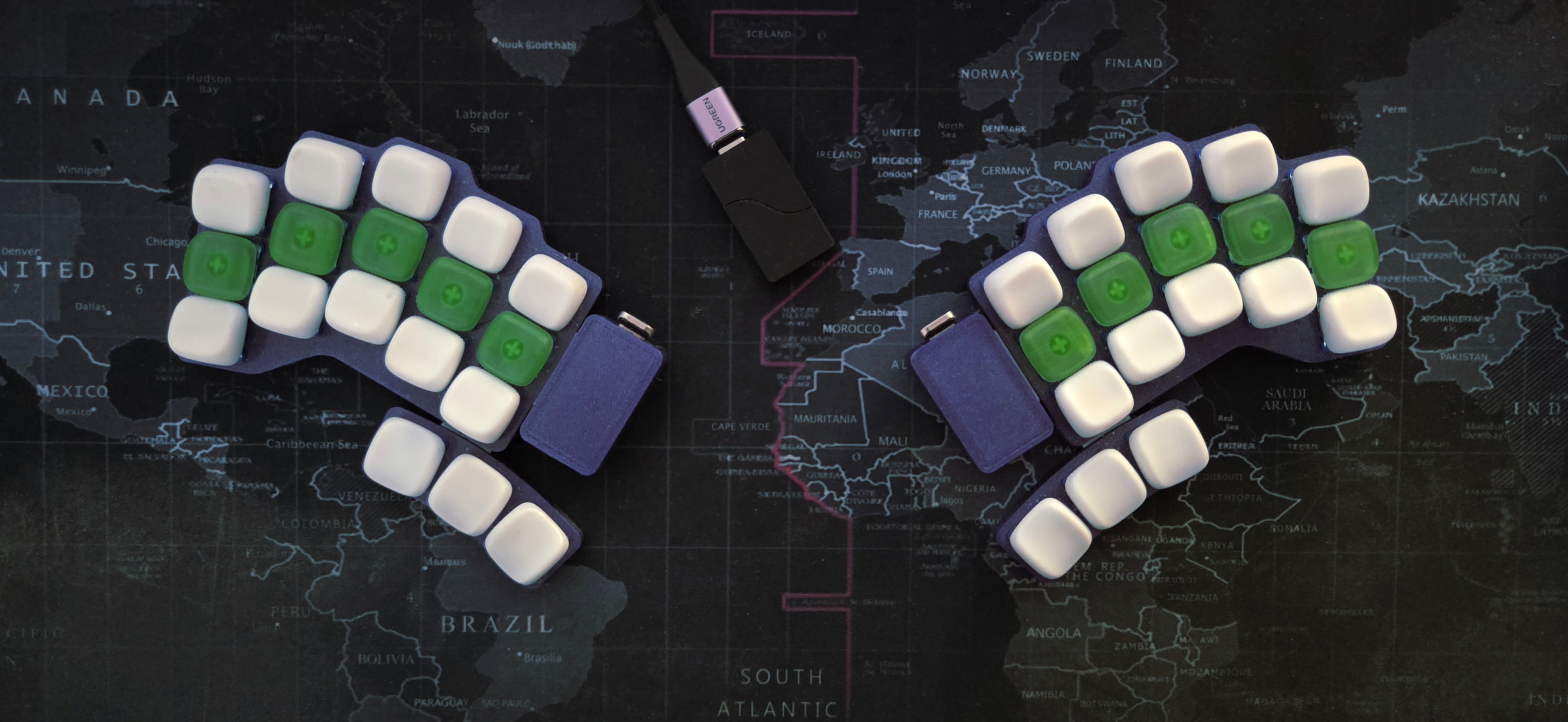
Беспроводная эргономичная сплит-клавиатура для тех, у кого лапки (:
Особенности:
Структура репозитория:
| Директория | Описание |
|---|---|
| 3MF | Проект OrcaSlicer (для примера параметров печати) |
| Assets | Изображения и фото |
| Fusion | Проект Autodesk Fusion 360 |
| Gerbers | Gerber-файлы для производства плат |
| Guide | Описание процесса сборки |
| KiCad | Проект KiCad (схема, плата, компоненты) |
| STL | 3D-модели частей корпуса |
Ссылки на актуальные прошивки:
Следуйте инструкциям в README.md репозитория с RMK прошивкой.
Используйте вариант подключения direct-pin, описанный в lapka_wellum36_left.overlay и lapka_wellum36_right.overlay.
Откройте GitHub Actions и найдите последний успешно собранный билд ветки lapka-36.
В нём будет артефакт сборки firmware.zip, который содержит все нужные для прошивки файлы.
Тестовая прошивка расположена в ветке lapka-36-test. В ней всего один слой и клавиши на тамб-кластере заменены на F1-F6. Это позволит увидеть нажатия клавиш на key-test.ru.
Wireless ergonomic split keyboard for those who have paws (:
Peculiarities:
Repository structure:
| Directory | Description |
|---|---|
| 3MF | OrcaSlicer project files (printing parameters example) |
| Assets | Images and photos |
| Fusion | Autodesk Fusion 360 project |
| Gerbers | Gerber-files for PCB production |
| Guide | Build guide |
| KiCad | KiCad project (schematics, PCB design, components) |
| STL | 3D-models of case parts |
Links to the current firmwares:
Follow the instructions in the README.md file of the RMK firmware repository.
Use direct pin layout, described in lapka_wellum36_left.overlay and lapka_wellum36_right.overlay.
Open GitHub Actions and find latest successful build of branch lapka-36.
In that build you'll find artifact firmware.zip, which contain all the neccessary firmware files.
Test firmware is located in branch lapka-36-test. There are single layer with F1-F6 keys on the thumb-cluster. That will help to see keypresses on the key-test.ru.
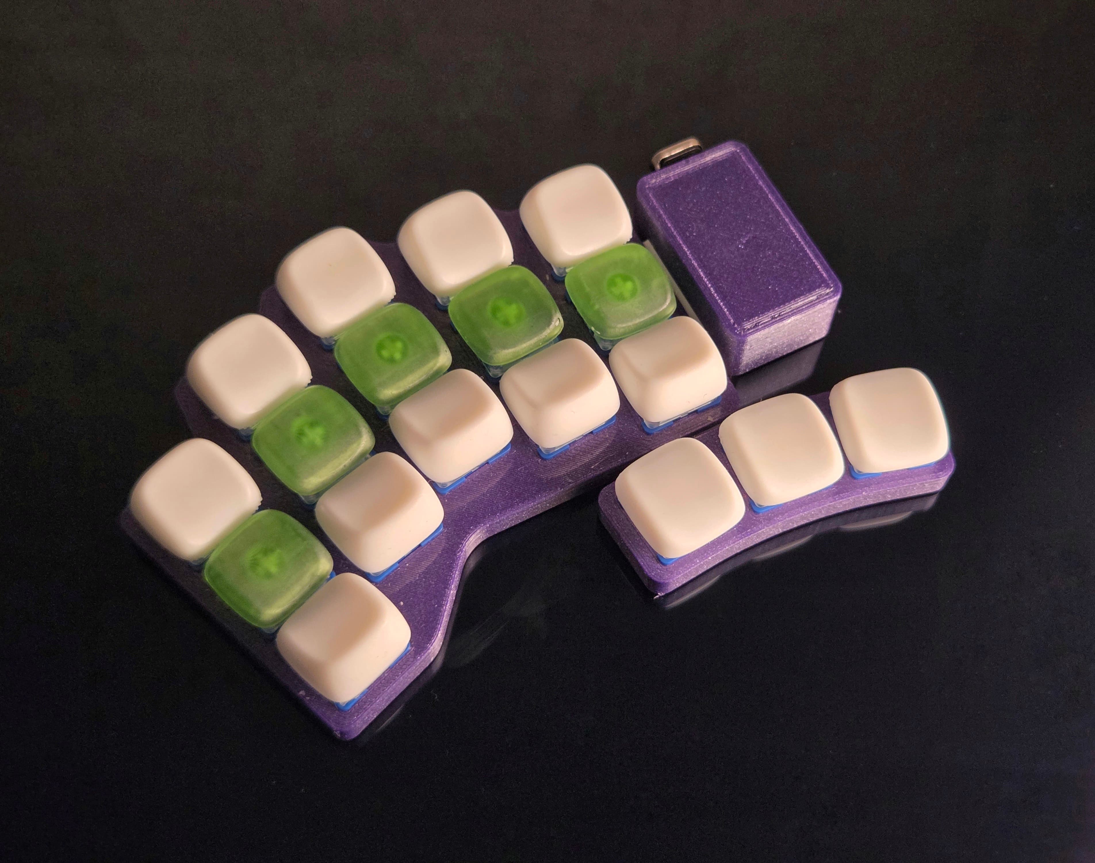
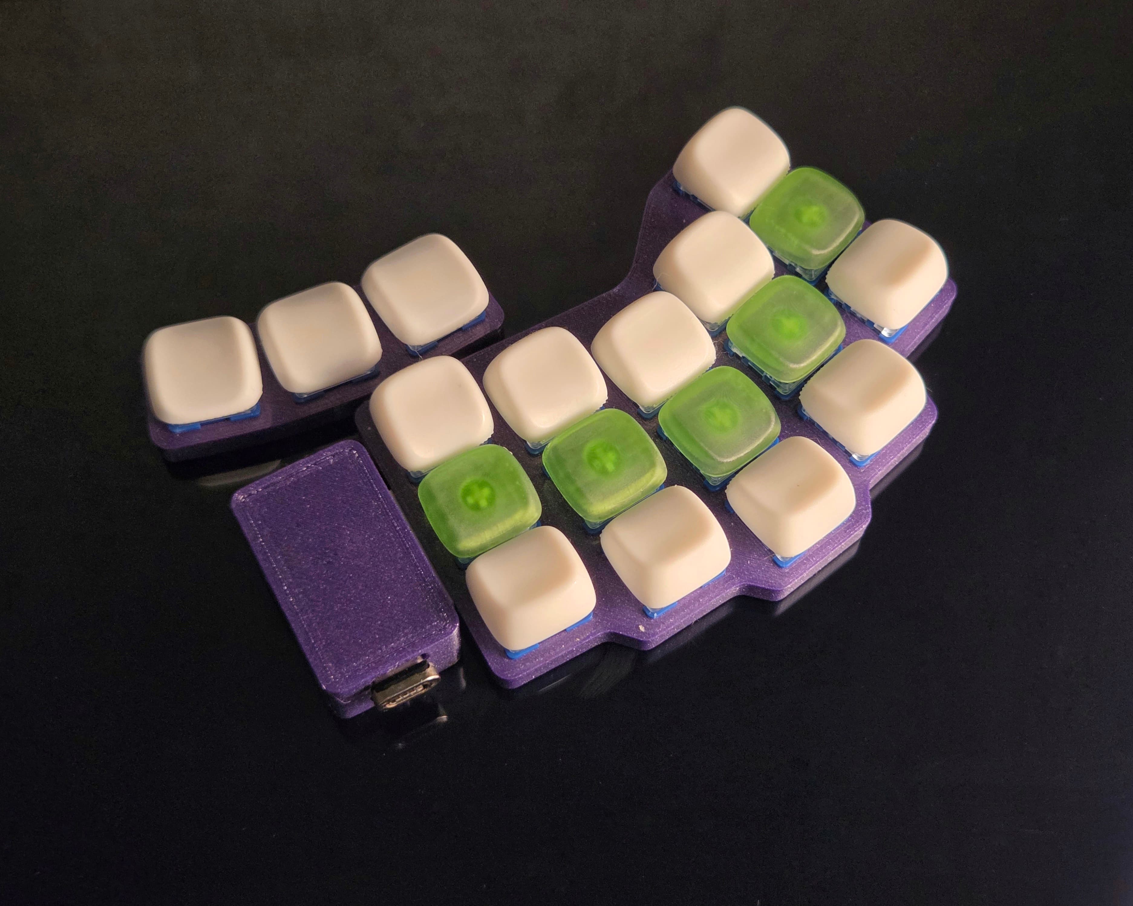
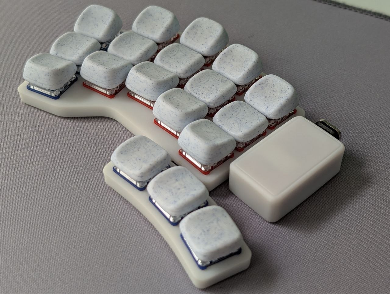
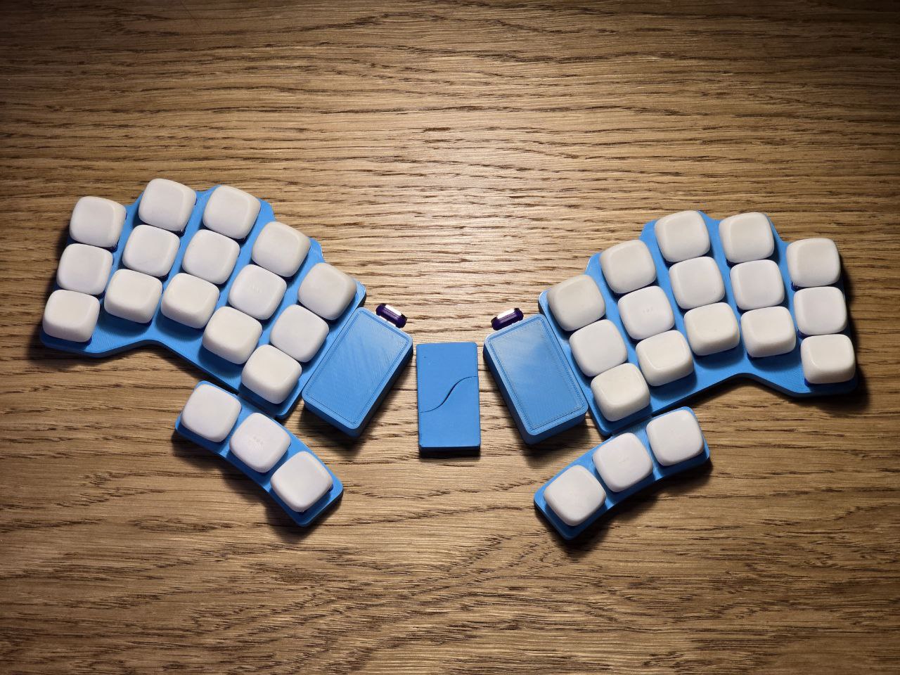
by Иосиф Правец
| Qty | Value | Footprint | References |
|---|---|---|---|
| 18 | ~ | PCM_Switch_Keyboard_Kailh:SW_KLPv2_DS | SW1, SW2, SW3, SW4, SW5, SW6, SW7, SW10, SW11, SW12, SW13, SW14, SW15, SW16, SW17, SW18 +2 |
| 1 | ~ | Library:SuperMini NRF52840 | U2 |
The 19 most common of 21 parts.
braindefender/lapka
Wireless ergonomic split keyboard for those who have paws (:

gusmanb/logicanalyzer
24 channel, 100Msps logic analyzer hardware and software

mntmn/amiga2000-gfxcard
MNT VA2000, an Open Source Amiga 2/3/4000 Graphics Card (Zorro II/III), written in Verilog


hackclub/OnBoard
💡 Join 1,000 teenagers and make your first PCB with a $100 grant!

drandyhaas/KiCadRoutingTools
A set of Python/Rust tools to aid routing in KiCad

Arrow-air/project-quiver
Project Quiver documentation, designs, and project artifacts.


It measures 130.3 × 85.3 mm and has 2 copper layers, 1.6 mm thick.
21 parts. The full list of its parts is on this page, with links to each part's symbol and footprint where PCBKit's library has them.
From the braindefender/lapka repository on GitHub, at the commit this page was made from: the board is KiCad/Archived/Lapka_ChocV2_Solder.kicad_pcb and its schematic KiCad/Archived/Lapka.kicad_sch. PCBKit opens the board in the browser, with nothing to install.
Its repository publishes it under the CC-BY-SA-4.0 licence: you may reuse it on that licence's terms (keep the author's notice, and for a copyleft licence share your changes alike).