
2 layers97.2 × 59.1 mm
ArmLEDsPrototype
hackclub/OnBoard
💡 Join 1,000 teenagers and make your first PCB with a $100 grant!
35 parts915

 boert/KC85__M062.2
TTL-Version des Speichermodul M062 für den KC85/3..4..5
M062.2 is an open-source printed circuit board by boert, from the boert/KC85__M062.2 repository on GitHub, published under the GPL-3.0 licence. It is a 2-layer board of 114.5 × 122.5 mm with 35 parts on 100 nets, routed with 1,350 tracks and 122 vias.
It is built around the SA39-11GWA. Its parts include 12 ICs, 9 resistors, 7 capacitors, 2 connectors and 1 crystal. It belongs with the retro computing and games boards of this library.
TTL-Version des Speichermodul M062 für den KC85/3..4..5 mit 32 kByte RAM (nichtflüchtig) oder 64 kByte EPROM
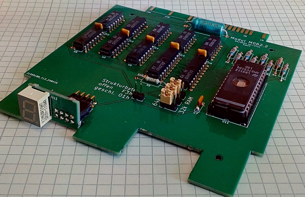
Um die Erweiterung der EPROM-Generator-Software 1 zu testen, wurde eine passende Hardware benötigt. Das M062 von E. Müller ist ein Speichermodul für den KC85 aus Mühlhausen, das entweder mit einem EPROM (64 kByte) oder einem nichtflüchtgen SRAM (32 kByte) bestückt werden kann. Durch den Einsatz eines CPLD werden im Original nur vier Schaltkreise benötigt.
Die hier vorgestellte Lösung entstand auf Basis einer Schaltungsbeschreibung in VHDL.
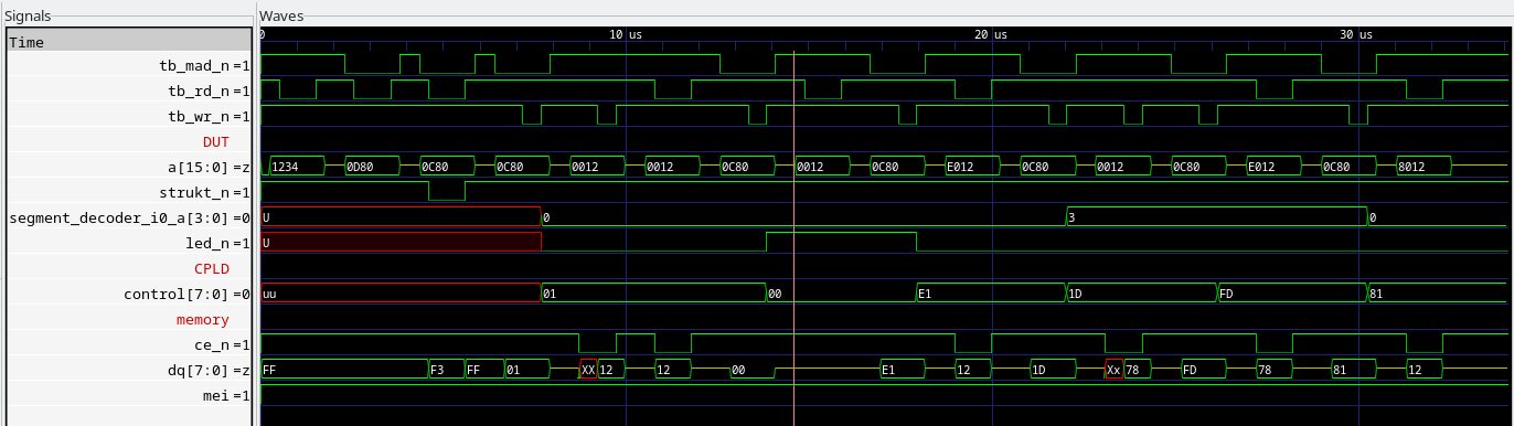 Mit Hilfe von yosys 2 und dem ghdl-plugin 3 ist es möglich aus der Schaltungsbeschreibung eine Netzliste zu erzeugen, die Elemente aus einer bereitgestellten TTL-Bibliothek verwendet.
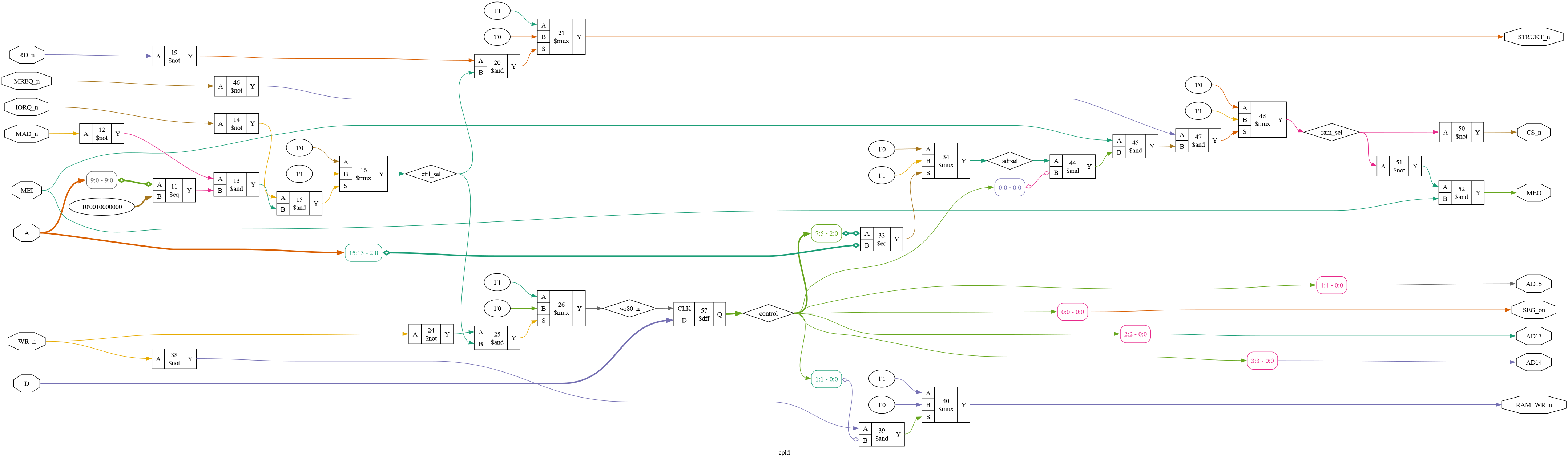
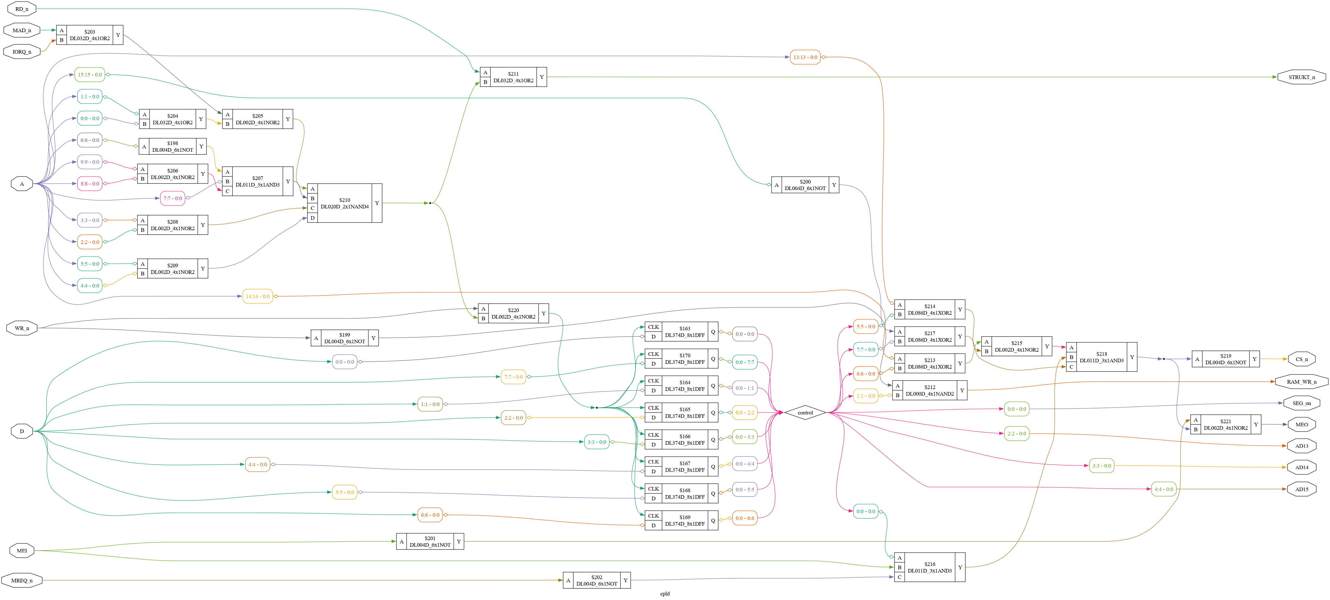
Diese Netzliste wurde als Basis für den Schaltplan herangezogen. Inklusive Speicher werden nun elf Schaltkreise benötigt.
Änderungen gegenüber dem Original
Übernommen wurde die Idee mit der kleinen Zusatzplatine für die Segmentanzeige.
Das Steuerbyte ist wie folgt aufgebaut:
| Bit | 7 | 6 | 5 | 4 | 3 | 2 | 1 | 0 |
|---|---|---|---|---|---|---|---|---|
| Bedeutung | A | A | A | S | S | S | W | M |
Das Speichermodul kann aus dem System CAOS mit dem Befehl SWITCH geschaltet werden.
| Bit 7 | Bit 6 | Bit 5 | Adressauswahl A |
|---|---|---|---|
| 0 | 0 | 0 | 0000h |
| 0 | 0 | 1 | 2000h |
| 0 | 1 | 0 | 4000h |
| 0 | 1 | 1 | 6000h |
| 1 | 0 | 0 | 8000h |
| 1 | 0 | 1 | A000h |
| 1 | 1 | 0 | C000h |
| 1 | 1 | 1 | E000h |
| Bit 4 | Bit 3 | Bit 2 | Segment S |
|---|---|---|---|
| 0 | 0 | 0 | 0 |
| 0 | 0 | 1 | 1 |
| 0 | 1 | 0 | 2 |
| 0 | 1 | 1 | 3 |
| 1 | 0 | 0 | 4 |
| 1 | 0 | 1 | 5 |
| 1 | 1 | 0 | 6 |
| 1 | 1 | 1 | 7 |
Die Segmente 4 bis 7 existieren nur bei Bestückung mit 64 kByte EPROM.
| Bit 1 | Schreibschutz W |
|---|---|
| 0 | aktiv (read only) |
| 1 | inaktiv (read write) |
| Bit 0 | Modulzustand M |
|---|---|
| 0 | inaktiv |
| 1 | aktiv |
Angenommen das Modul M062.2 steckt im Modulschacht 0C.
Um das Segement 3 im Speicher auf Adresse 4000h im Modus Schreiben/Lesen zu aktivieren, wird der CAOS-Befehl "SWITCH C 4F" verwendet.
Um das Segement 7 im Speicher auf Adresse C000h im Modul Nur-Lesen zu aktivieren, wird der CAOS-Befehl "SWITCH C DD" verwendet.
| Qty | Value | Footprint | References |
|---|---|---|---|
| 8 | 120 | Resistor_THT:R_Axial_DIN0309_L9.0mm_D3.2mm_P15.24mm_Horizontal | R1, R2, R3, R4, R5, R6, R7, R8 |
| 6 | 100n | Capacitor_THT:C_Rect_L7.0mm_W2.0mm_P5.00mm | C2, C3, C4, C5, C6, C7 |
| 2 | DL002D | Package_DIP:DIP-14_W7.62mm_LongPads | U4, U9 |
| 1 | 0-7/0-3 | Connector_PinHeader_2.54mm:PinHeader_1x03_P2.54mm_Vertical | JP1 |
| 1 | 10k | Resistor_THT:R_Axial_DIN0309_L9.0mm_D3.2mm_P15.24mm_Horizontal | R9 |
| 1 | 22µF | Capacitor_THT:CP_Axial_L18.0mm_D8.0mm_P25.00mm_Horizontal | C1 |
| 1 | 7-Segment (in) | Connector_PinHeader_2.54mm:PinHeader_2x04_P2.54mm_Vertical | J2 |
| 1 | 7-Segment (out) | Connector_PinSocket_2.54mm:PinSocket_2x04_P2.54mm_Horizontal | J1 |
| 1 | D345D | Package_DIP:DIP-16_W7.62mm_LongPads | U5 |
| 1 | DL004D | Package_DIP:DIP-14_W7.62mm_LongPads | U2 |
| 1 | DL011D | Package_DIP:DIP-14_W7.62mm_LongPads | U8 |
| 1 | DL020D | Package_DIP:DIP-14_W7.62mm_LongPads | U3 |
| 1 | DL032D | Package_DIP:DIP-14_W7.62mm_LongPads | U1 |
| 1 | DL086D | Package_DIP:DIP-14_W7.62mm_LongPads | U6 |
| 1 | DL374D | Package_DIP:DIP-20_W7.62mm_LongPads | U10 |
| 1 | DL540D | Package_DIP:DIP-20_W7.62mm_LongPads | U7 |
| 1 | F3h/01h | Connector_PinHeader_2.54mm:PinHeader_1x02_P2.54mm_Vertical | JP2 |
| 1 | KC85_Modulsteckverbinder_M062 | pcb_kicad:KC85_Modul_M062 | X1 |
| 1 | Pin1 | Connector_PinHeader_2.54mm:PinHeader_1x03_P2.54mm_Vertical | JP4 |
| 1 | Pin27 | Connector_PinHeader_2.54mm:PinHeader_1x03_P2.54mm_Vertical | JP3 |
| 1 | SA39-11GWA | Display_7Segment:Sx39-1xxxxx | U12 |
| 1 | U27512 | Package_DIP:DIP-28_W15.24mm_Socket_LongPads | U11 |
hackclub/OnBoard
💡 Join 1,000 teenagers and make your first PCB with a $100 grant!


ozel/DIY_particle_detector
A mobile low-cost spectrometer for measuring radioactivity and the energy of ionising radiation like alpha particles and electrons

Seeed-Studio/OSHW-reCamera-Series
reCamera is a series of open-source AI cameras.


It measures 114.5 × 122.5 mm and has 2 copper layers, 1.6 mm thick.
35 parts, built around the SA39-11GWA. The full list of its parts is on this page, with links to each part's symbol and footprint where PCBKit's library has them.
From the boert/KC85__M062.2 repository on GitHub, at the commit this page was made from: the board is pcb_kicad__Prototyp/M062.2.kicad_pcb and its schematic pcb_kicad/M062.2.kicad_sch. PCBKit opens the board in the browser, with nothing to install.
Its repository publishes it under the GPL-3.0 licence: you may reuse it on that licence's terms (keep the author's notice, and for a copyleft licence share your changes alike).