

2 layers151.1 × 95.3 mm
LED Panel
Plasmarobo/Disarmed
Heavily inspired by Keep Talking and Nobody Explodes and Bomb Corp.
38 parts1

Electronics and software to help time delays in camera exposure based on NEXTA
Nexta is an open-source printed circuit board by bluthen, from the bluthen/exposure_timing repository on GitHub, published under the GPL-3.0 licence. It is a 2-layer board of 88.9 × 53.3 mm with 29 parts on 104 nets, routed with 254 tracks and 20 vias.
It is built around the LTA-1000G.
A lot of this project is based off New EXposure Timing Analyser (NEXTA): a GNSS-based precise timer, as presented in the wonderful paper Reaching sub-millisecond accuracy in stellar occultations and artificial satellites tracking[arvix] (local mirror) by authors K. Kamiński , C. Weber , A. Marciniak , M. Żołnowski & M. Gędek.
The goals are to design electronics and boards to make this easy to use.
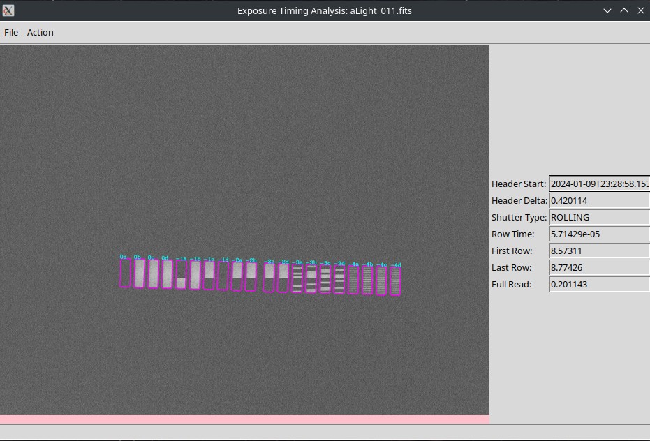 Showing the simple GUI after time analysis has been run. Header delta is what should be added to the time stamp to make it more accurate.
Please note that individual files in the repository have different licenses. For example the NEXTA microcontroller code is under CC BY-SA 4.0 and the some of the analysis software is under the GNU GPL 3.
There can be delays, or accuracy issues between when the camera is told to start it's exposure and when it actually does. This can be important for time critical applications. Also of importance is the time difference for each row in CMOS cameras with a rolling shutter.
In particular the timing application originally of interest is imaging fast time critical astronomical events. Such events include, LEO satilite, astroid transits, fast NEOs.
A better introduction is described in the paper listed above.
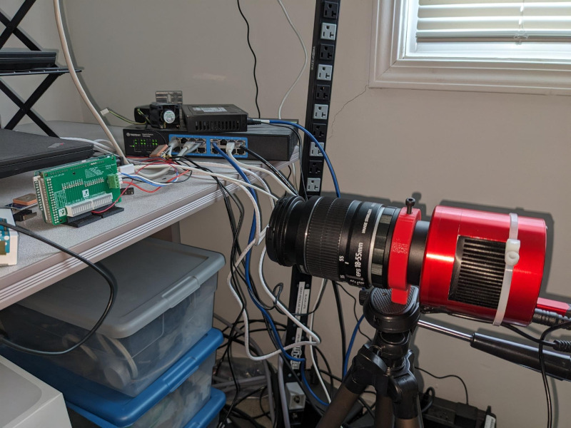
There is a still a lot to do, this project is in it's early stages. Check out the issue tracker and, feel free to contribute.
If you are interested in this project, you may be also interested in the following.
| Qty | Value | Footprint | References |
|---|---|---|---|
| 20 | R | Resistor_SMD:R_0805_2012Metric | R1, R2, R3, R4, R5, R10, R11, R12, R13, R14, R15, R16, R17, R18, R19, R20 +4 |
| 2 | LTA-1000G | Display:HDSP-4850 | BAR1, BAR2 |
| 1 | Arduino_Due_Shield | PCM_arduino-library:Arduino_Due_Shield | A1 |
| 1 | Screw_Terminal_01x05 | Connector_PinHeader_2.54mm:PinHeader_1x05_P2.54mm_Vertical | GPS1 |
The 24 most common of 29 parts.
Plasmarobo/Disarmed
Heavily inspired by Keep Talking and Nobody Explodes and Bomb Corp.

gusmanb/logicanalyzer
24 channel, 100Msps logic analyzer hardware and software

VoronDesign/Voron-Hardware
Cool Hardware designed by the Voron Design group

hoglet67/RGBtoHDMI
Bare-metal Raspberry Pi project that provides pixel-perfect sampling of Retro Computer RGB/YUV video and conversion to HDMI

hackclub/OnBoard
💡 Join 1,000 teenagers and make your first PCB with a $100 grant!

OLIMEX/DIY-LAPTOP
Do It Yourself Open Source Hardware and Software Modular Hacker's Friendly Laptop

UtilitechAS/amsreader-firmware
ESP8266 and ESP32 compatible firmware to read, interpret and publish data to MQTT from smart electrical meters, both DLMS and DSMR is supported

It measures 88.9 × 53.3 mm and has 2 copper layers, 1.6 mm thick.
29 parts, built around the LTA-1000G. The full list of its parts is on this page, with links to each part's symbol and footprint where PCBKit's library has them.
From the bluthen/exposure_timing repository on GitHub, at the commit this page was made from: the board is hardware/pcb/nexta.kicad_pcb and its schematic hardware/pcb/nexta.kicad_sch. PCBKit opens the board in the browser, with nothing to install.
Its repository publishes it under the GPL-3.0 licence: you may reuse it on that licence's terms (keep the author's notice, and for a copyleft licence share your changes alike).