2 layers97.1 × 97 mm

 blurbler2/TL082CP
Abschlussaufgabe der Lehrveranstaltung "Computerunterstützter Schaltungs- und Systementwurf" (CAE).
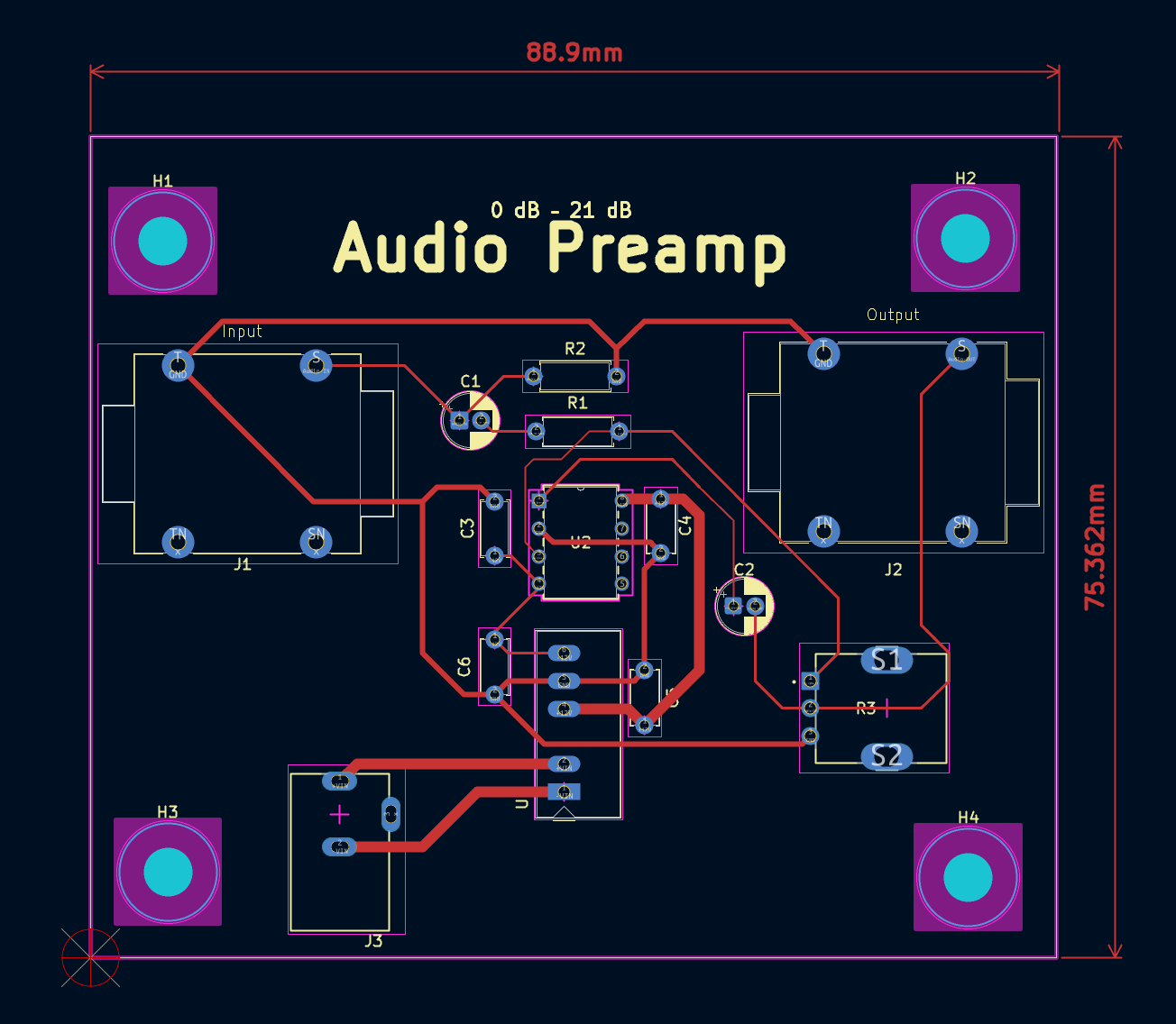
TL082CP is an open-source printed circuit board by blurbler2, from the blurbler2/TL082CP repository on GitHub. It is a 2-layer board of 88.6 × 75.4 mm with 18 parts on 15 nets, routed with 85 tracks and 0 vias.
It is built around the TMR 1-1222, TL082 and PJ-102A, with the PT01-D130D-B503 among its other parts. Its parts include 6 capacitors, 3 resistors, 3 connectors and 2 ICs.


Abschlussaufgabe der Lehrveranstaltung "Computerunterstützter Schaltungs- und Systementwurf" (CAE).
Bauteil: TL082CP — Dual JFET-Input Operational Amplifier (Texas Instruments BI-FET II™)
Bauteil: TL082CP — Dual JFET-Input Operational Amplifier
Bauform: Frei wählbar (gewählt: PDIP-8)
Anwendung: Audio-Vorverstärker (Gitarren-Pedal)
Abgabe: Moodle-Kurs bis spätestens 05.07.2026, 23:55 Uhr
TL082CP/
├── kicad/                          # KiCad Projekte
│   ├── TL082CP/                    # Hauptprojekt (Gitarren-Pedal)
│   │   ├── TL082CP.kicad_pro
│   │   ├── TL082CP.kicad_sch      # Top-Level Schematic
│   │   ├── audio-vorverstaerker-TL082CP.kicad_sch  # Audio Amp Schaltung
│   │   ├── audio_signal.kicad_sch  # Signalweg
│   │   ├── power.kicad_sch         # Stromversorgung
│   │   └── TL082CP.kicad_pcb       # PCB Layout
│   │
│   ├── TL082-smd/                  # SMD Version (SOIC-8)
│   │   ├── TL082.kicad_sym
│   │   └── SOIC127P600X175-8N.kicad_mod
│   │
│   ├── ul_TL082CP-NOPB/            # Ultra Librarian Import
│   │   └── KiCADv6/
│   │       ├── 2026-07-03_18-03-43.kicad_sym
│   │       └── footprints.pretty/P8_TEX.kicad_mod
│   │
│   ├── 1_own_TL082CP.pretty/       # Eigene Footprints
│   │   ├── P8_TEX.kicad_mod
│   │   └── SOIC127P600X175-8N.kicad_mod
│   │
│   ├── NEUTRIKJKS/                 # Neutrik Audio-Jack Projekte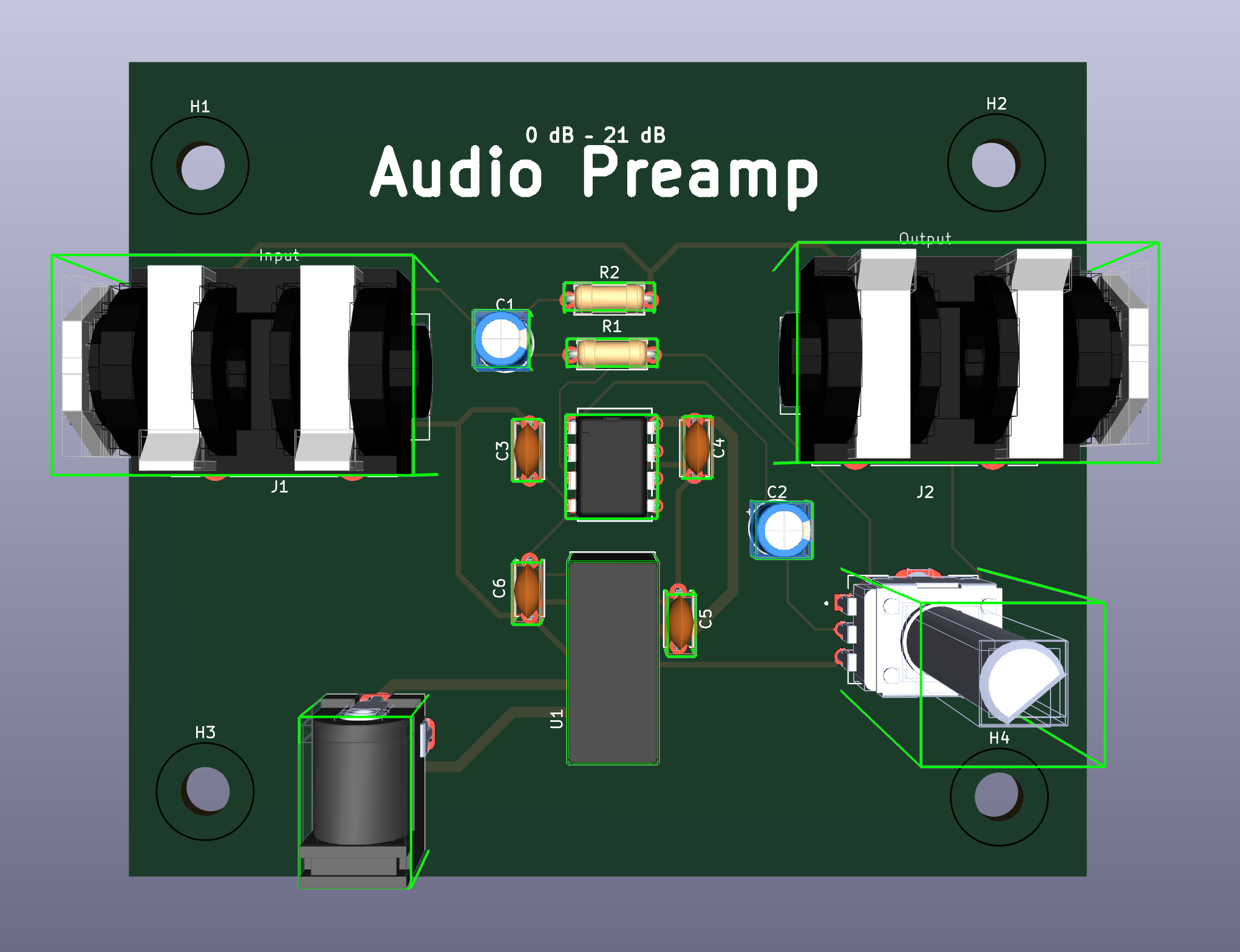
| Datei | Beschreibung |
|---|---|
kicad/documentation.md | Vollständige Dokumentation des Gitarren-Pedals |
kicad/idee.md | Schaltungsidee mit ASCII-Schema und BOM |
docs/tl082.pdf | Datenblatt (Texas Instruments) |
docs/application-note.pdf | Application Note |
ltspice/ | LTSpice Simulationen (Slew Rate, Offset Voltage) |
Die Dokumentation (abgabe.md) lässt sich mit Pandoc + XeLaTeX in ein druckbares PDF umwandeln.
brew install pandoc (macOS) bzw. apt install pandoc (Linux) bzw. https://pandoc.orgabgabe.md → PDFpandoc abgabe.md \
--pdf-engine=xelatex \
-V lang=de \
-V geometry:margin=2.5cm \
-V fontsize=11pt \
-V colorlinks=true \
-o abgabe.pdf-V lang=de empfohlen.Eine Massefläche muss auf einem Kupfer-Layer erstellt werden, nicht auf User.1.
Zone löschen — Falls eine Zone auf User.1 existiert: Zone auswählen → Delete
Neue Zone auf B.Cu erstellen
Place → Zone (Shortcut P Z)B.Cu wählenNet: → GND auswählenZone connection: → Thermal Relief (empfohlen)Zone zeichnen
Fill Zone oder B drückenAlle Netze neu zeichnen
Tools → Rebuild All Zones oder Shift+BDRC prüfen
Tools → Design Rule Check → Start — keine GND-Fehler sollte angezeigt werden** Gerber neu exportieren**
File → Fabrication Outputs → Gerber — Layer B.Cu muss enthalten seinFile → Fabrication Outputs → Drill Files — Bohr-Dateien aktualisierenUser.1?User.1 ist eine Dokumentationsebene — Flächen darauf sind nur optisch sichtbar, elektrisch haben sie keine Funktion. Die Ground Plane muss auf B.Cu (oder F.Cu) liegen, damit sie tatsächlich mit dem GND-Netz verbunden ist.
Während der Arbeit an diesem Projekt wurden folgende Probleme identifiziert:
Die Mounting-Holes im PCB wurden nach dem ersten Layout nachträglich neu positioniert:
Mounting-platform-for-PCB.scad) wurde entsprechend angepasstBeim Exportieren der Bohr-Dateien über die KiCad GUI wurde ☑ Use drill file origin gesetzt — dennoch wurden die Koordinaten als absolute (PCB-Koordinatensystem) exportiert, nicht relativ zur Drill Origin.
.drl-Datei zeigt FORMAT={-:-/ absolute / metric / decimal}--drill-origin plot) wurde noch nicht getestetDie Ground Plane Zone lag zunächst auf User.1 — einer Dokumentationsebene, nicht auf einem Kupfer-Layer.
User.1 sind nur optisch sichtbar, elektrisch keine FunktionB.Cu mit Netz GND erstellenZIP-File mit allen geforderten Unterlagen, Moodle-Kurs "CUE SS2026 – AE27", bis spätestens 05.07.2026, 23:55 Uhr.
| Qty | Value | Footprint | References |
|---|---|---|---|
| 4 | 100nF | Capacitor_THT:C_Disc_D5.0mm_W2.5mm_P5.00mm | C3, C4, C5, C6 |
| 4 | MountingHole_4.5mm | MountingHole:MountingHole_4.5mm | H1, H2, H3, H4 |
| 2 | 10µF | Capacitor_THT:CP_Radial_D5.0mm_P2.00mm | C1, C2 |
| 2 | AudioJack2_Switch | Connector_Audio:Jack_6.35mm_Neutrik_NMJ4HCD2_Horizontal | J1, J2 |
| 1 | 1Meg | Resistor_THT:R_Axial_DIN0207_L6.3mm_D2.5mm_P7.62mm_Horizontal | R2 |
| 1 | 4,7k | Resistor_THT:R_Axial_DIN0207_L6.3mm_D2.5mm_P7.62mm_Horizontal | R1 |
| 1 | PJ-102A | 1_own_PJ-102A:CUI_PJ-102A | J3 |
| 1 | PT01-D130D-B503 | 1_own_PT01-D130D-B503:TRIM_PT01-D130D-B503 | R3 |
| 1 | TL082 | 1_own_TL082CP:P8_TEX | U2 |
| 1 | TMR_1-1222 | Converter_DCDC:Converter_DCDC_TRACO_TMR-1-xxxx_Dual_THT | U1 |
It measures 88.6 × 75.4 mm and has 2 copper layers, 1.6 mm thick.
18 parts, built around the TMR 1-1222, TL082, PJ-102A and PT01-D130D-B503. The full list of its parts is on this page, with links to each part's symbol and footprint where PCBKit's library has them.
From the blurbler2/TL082CP repository on GitHub, at the commit this page was made from: the board is kicad/TL082CP/TL082CP.kicad_pcb and its schematic kicad/TL082CP/TL082CP.kicad_sch. PCBKit opens the board in the browser, with nothing to install.
Its repository states no licence, so its author keeps all rights: ask blurbler2 before reusing the design.

CodapopKSP/UntitledSpaceCraft
The entire project files from the Untitled Space Craft brand of Kerbal controllers.


amigalisa/RGBSvideoConverter
RGB to SVideo converter for Amiga computers

stefanofinetti/MF_OverHead_Panel
Complete project for the Airbus A319/320/321/330 OverHead Panel

